When we engineers look at the complexity of system design these days, we are challenged with cramming more functions into a smaller space, while consuming less power, and doing all of this in much shorter design cycles.
Efficient and effective analog design has always been a significant roadblock to hitting our deadlines; generally speaking, digital design and verification is much easier. This has certainly been true in our experience, which has involved spending the last 30 years learning the “art” of mixed-signal design.
Unfortunately, the ability to overcome the size and performance constraints of analog blocks is directly proportional to the mixed-signal engineer’s experience. Learning this art can take a lifetime. The time investment not only strains design cycles, but also hurts creativity, and it can be an impediment to cultivating a young, robust labor pool. The vast number of new graduates going into digital design as opposed to analog design is evidence of this. As a result, not much has truly been done to improve the underlying fabric of analog architecture and address inherent problems over the last 20 years.
As our end products get more complex, the more important analog design efficiency becomes to the overall system. Additionally, the more “sensory” our end products become, the more analog-to-digital (ADC) converters are required. And the more portable these end products become, the more important is the efficiency of those ADCs. As we looked over the wall at our digital design colleagues, we often wondered if the underlying analog ADC design could ever be as efficient as digital design. Now it can be.
Programmable digital devices, led by FPGAs, have exploded in popularity as costs have come down and performance has increased. Some experts suggest that the breakeven point between ASIC and FPGA for certain applications is around 220,000 units. Additionally, shrinking product life cycles are making higher volumes more difficult.
Even with the explosion in popularity, FPGAs still only account for 2% of the overall semiconductor market. Two recent articles on EE Times highlight this paradox. One, Using FPGAs in mission critical systems, highlights how FPGAs are being used for high reliability applications such as aerospace, automotive and medical, while the other, Programmable ICs: The Next Innovation Engine, identifies and describes the most fundamental challenges to continuing the growth path of FPGAs. Challenge #1 in the latter article is mixed-signal circuit integration. Specifically, the article mentions that ADCs, DACs, and power circuits will need to be integrated to drive the next wave of FPGA evolution.
Originally, Stellamar set out to replicate in the ADC world what the Sigma-Delta DAC did to the DAC world. Most traditional DACs gave way to the Sigma-Delta version because of its mostly digital nature and ease of integration. If the same could be done for ADCs, then the industry would have a robust solution for the integration of ADCs into FPGAs. It was this challenge that sparked our innovation to create the most flexible, cost-effective way to implement analog functions in digital fabric.
An A2D without the A
At Stellamar, we have created an All-Digital ADC requiring no analog block. By using an LVDS pin-pair, only a few passive components, and some specialized proprietary signal processing, an analog Sigma-Delta ADC performance can be replicated with digital-only library cells. This proprietary technology allows All-Digital ADCs to reap all the benefits that digital design has over its analog counterparts to realize [for the ADC function(s)]:
- 50% lower power on average
- 68% smaller area on average
- Process technology independence
- Reduced risk and cycle time
- Digital integration and synthesis
- Easier radiation-hardened design
The difference can easily be seen using the simple block diagrams shown in Figure 1 (A traditional ADC interface) and Figure 2 (An All-Digital ADC interface).

In the traditional analog ADC approach, the good news is that creating the ADC is usually a vendor’s responsibility. This specialization of labor can get very high tolerances and performance. The bad news is that these ADCs are usually external and large. Multiple pins are needed to connect to an ASIC or FPGA. By not controlling the ADC development, designers trade off optimization for reduced design cycles. The vendor’s solution is most likely an overdesigned part for the system, which we gladly take because it is too much headache to design an optimized ADC.
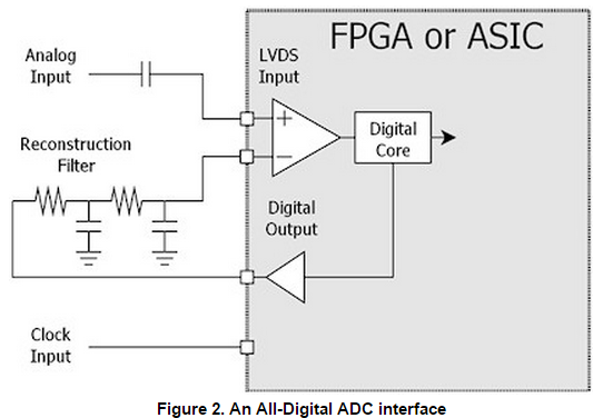
With this All-Digital approach, a designer does not have to use external ADCs, which can take up critical board space. The ADC is right is the digital fabric and is much easier to implement. The Digital ADC only uses 2 pins and a couple discrete components as depicted in Figure 2.
This means that you now have the ability to embed one or more ADCs in the digital fabric of your ASIC or FPGA, which is properly optimized for your application, and you have also reduced board space, complexity, and testing time, while increasing MTBF. This approach is much easier to implement and test, which can greatly enhance your ability to meet time to market.
For additional ADC functionality using the conventional approach, either more ADC chips would be added, or an analog multiplexer would have to be employed. By comparison, when using an All-Digital ADC solution, a designer can simply add additional All-Digital ADC IP blocks to take advantage of their size and power savings.
“Wait a minute,” you may be thinking, “you can’t do that. Analog is analog and digital is digital. It doesn’t work that way. I don’t believe this can be done.” This is the normal first reaction of just about everyone we’ve talked to. The best way to answer this is by means of the following video clip, which demonstrates the real capability of an All-Digital ADC using an audio example:
The following are the typical frequency response plots for an ADC with a bandwidth of 20 kHz. The plots show an output with two different amplitudes of a 15 kHz input frequency. The first has an amplitude of 1.8 Vpp while the second is 60 dB lower with an amplitude of 1.8 mVpp.

The power estimate for a Xilinx Spartan 3AN which contains a single channel, 12 bit, 20 kHz bandwidth ADC with a typical digital filter, an I2S interface, and a SPDIF interface is 6mW. The power will vary among FPGA vendors and FPGA families. This power number will also depend largely on customer requirements.
Deliverables
All-Digital ADCs are suitable for ASIC or FPGA applications. Current FPGA evaluation boards are available for purchase on our website (www.stellamar.com); these show 11 bits of resolution over a 20 kHz bandwidth for standard resolution, and 14 bits over 500 Hz for higher resolution applications.
A purchased All-Digital ADC block can be specifically optimized just about anywhere below those thresholds. ASIC performance implementations can be markedly improved due to better control over mixed-signal rules. Resolution and sample rates are driven by customer requirements. Stellamar will work with the customer to deliver customized RTL that best suits those requirements. The encrypted RTL will also allow the customer to target their desired technology and foundry. With the encrypted RTL, Stellamar provides a detailed Implementation Guide, and offers customer support through implementation.
Applications
As the above video shows, an All-Digital ADC can easily handle voice-type applications, and the current performance covers a host of other applications including the following:
- Sensors: temperature, pressure, voltage, current, acceleration
- Touch screen integration
- Voice and high quality voice
- Wireless headsets
- Hearing aids
- Medical devices
- Motor control
- Radiation-hard aerospace needs
FPGA implementation example
FPGAs have been used for low-volume type production systems that need to provide custom functionality. FPGAs may be used in mission-critical applications especially in industrial monitoring and aerospace where economies just aren’t there for ASIC implementations.
For example, FPGAs are used extensively in commercial and military satellites for system health monitoring; measuring voltage, current, temperature, pressure etc. Since FPGAs and ADCs come in both commercial and rad hard varieties, together they provide a much needed service that can be customized without the cost of producing an ASIC. The problem is that in both commercial and military applications, the ADCs are external to the digital fabric, taking up space, power and impacting reliability. These critical factors are all high on the priority list when a satellite is designed.
With an All-Digital ADC, designers can now use the FPGA digital fabric, thereby reducing board space, weight, power, and increasing reliability while still providing the same functionality. Furthermore, additional monitoring would be enabled without increasing weight and power. The reduction of weight, power, and increased reliability amounts to lowering not only the cost of the satellite itself but the insertion costs as well. With increased reliability, the mean time before failure (MTBF) will increase, resulting in longer satellite lifetime.
ASIC implementation example
The most obvious examples for ASIC applications are where ADCs are a large part of the system and that system needs to be small and mobile; for example, a Bluetooth headset. In the typical Bluetooth headset there are roughly 4 ADCs for noise cancellation and one ADC for voice. These designs are driven by consumer demand for more talk time and smaller products.
If All-Digital ADCs replaced the analog ADCs for noise cancellation and voice, the design could actually save at least 50% of the power used by the ADCs in the current Bluetooth implementation while reducing the total area associated with all the ADCs by 68%.
The result would be longer talk time and a smaller footprint with no loss in functionality or performance. We can create a fully-synthesizable All-Digital ADC, optimized and targeted to the customer’s system requirements, in a matter of weeks. Perhaps most appealing is that an All-Digital ADC is technology-independent and can take full advantage of a technology shrink without requiring any redesign. This will reduce risks and time to market, enable first pass success, and directly impact the bottom line from a cost-per-wafer perspective.
Radiation-hardening
Since the design of a traditional analog/mixed-signal rad-hard ADC is extremely difficult, expensive, and lengthy (typically over two years), only a few rad-hard ADCs are developed, and these few target applications requiring the highest conversion speed.
The same expensive ADCs are then used for lower-speed applications such as voltage measurements and pressure/ acceleration sensors on the system. This means that power is being wasted and system performance is not optimized. Digital ADCs targeting the low-speed applications could be quickly developed and embedded into the existing extra digital fabric in an ASIC. Mixed-signal FPGAs are large, expensive, and not optimized. If you have a radiation-hard/tolerant FPGA already on-board, why not use the remaining 2-3% of the gates to run an optimized rad-hard All-Digital ADC, and leave the “big boy ADC” powered off? You have not increased the number of parts, or board space, and now you’re optimized for power and you also have a configurable All-Digital ADC that you can repurpose for other applications.
Conclusion
Designers requiring ADC integration in either an FPGA or ASIC now have a simple, flexible and complete solution. With a Stellamar All-Digital ADC, most of the common bottleneck issues caused by ADC integration are removed. The result is an All-Digital ADC that can be easily embedded in any FPGA, not just large and expensive mixed-signal FPGAs, and that can be reprogrammed for different performance requirements.
All-Digital ADCs will also be much smaller and less power hungry for low power portable applications. Finally, an All-Digital ADC can be easily ported across process technologies without re-design to leverage the ASIC cost structure and realize bottom-line savings.
In the near future, engineers will be better able to integrate and synthesize other components previously thought to reside only in the analog domain. The All-Digital ADC is the first step