时钟 Clocks
为了进行时序分析,你必须指定时钟的周期或者设计中使用的时钟,以及可能的过渡时间,波形,延迟,不确定性,相对偏移,以及其他时序特性,如图1-9所示。时序分析将以上所有的时序特性考虑在内,以确定每种时序检查的最坏可能情形。指定时钟的命令叫做create_clock.
To perform timing analysis, you must specify the period of the clock or clocks used in the design and possibly the transition time, waveform, latency, uncertainty, relative skew, and other timing characteristics, as shown in Figure 1-9. The timing analysis takes all of these clock characteristics into account to determine the worst possible conditions for each type of timing check. The command for specifying clocks is create_clock.
图1-9 时钟特性
Figure 1-9 Clock Characteristics

如果在设计中使用了多个时钟,你必须指定这些时钟之间的关系,以便分析工具能够检查由一个时钟触发,由另一个时钟捕获的路径时序信息。默认情况下,工具认为在路径起始点发生(信号)启动事件后,下一个能够在路径终点发生的时间边沿应该能够捕获在路径终点的数据。任何与这个基本假设不符的异常都必须被看做时序异常。时序异常的例子包括:假路径、多周期路径、明确的最小延迟路径和最大延迟路径。
If multiple clocks are used in the design, you must specify the timing relationships between those clocks so that the analysis tool can check the timing of a path launched by one clock and captured by another. By default, the tool assumes that after the occurrence of a launch event at a path startpoint, the very next clock edge that can occur at the path endpoint should capture the data at the end of the path. Any exceptions to this basic assumption must be specified as timing exceptions. Some examples of timing exceptions are false paths,multicycle paths, and explicit minimum-delay paths and maximum-delay paths:
•假路径是设计中物理存在的路径,但由于逻辑电路配置,预期的数据序列,或者操作模式的原因,不会将数据从起始点传播到终点。
•多周期路径是一个设计上从触发到捕获需要超过1个时钟周期的路径
•最小延迟路径或最大延迟路径是一个必须满足设计者显式指定的带具体值的延迟约束的路径
一个时钟信号通常情况下对许多时序器件有着很大的扇出系数。因此,每个时钟通常实现为一个多级层次结构中组织的缓冲区的分支树。
时钟树综合通常运行在布局布线层,而不是在逻辑综合层。因为布局布线层提供了用于生成时钟树的内部连线长度信息。
为了在时钟树综合和布局之前执行时序分析,逻辑综合工具必须估计从时钟源到时序器件时钟引脚的延迟。
• A false path is a path that physically exists in the design but never propagates data from the startpoint to the endpoint due to the logic configuration, expected data sequence, or operating mode.
• A multicycle path is a path designed to take more than one clock cycle from launch to capture.
• A minimum-delay path or maximum-delay path is a path that must meet a delay constraint that you specify explicitly as a time value.
A clock signal typically has a very large fanout to many sequential devices. Therefore, each clock is usually implemented as a branching tree of buffers organized in a multilevel hierarchy. Clock tree synthesis is typically performed at the placement and routing stage, not at the logic synthesis stage, because placement and routing provide the interconnect length information needed to build the tree. To perform timing analysis before clock tree synthesis and layout, the logic synthesis tool must estimate the delays from the clock source to the clock pins of sequential devices.

输入与输出延迟
Input and Output Delays
时序分析工具通过比较起始点到终点的延迟与发射和捕获时钟边缘之间的时间跨度来确定路径的时间裕量。但是,对于从设计的输入处开始的路径,不能从设计的网表中确定数据到达的时间。这是因为外部发射时间和逻辑延迟是未知的。因此,要分析输入到寄存器的时间,必须将导致输入的外部时间条件指定为输入延迟。这个概念如图1-10所示。
The analysis tool determines the timing slack for a path by comparing the startpoint-to-endpoint delay with the time span between the launch and capture clock edges.However, for a path starting at an input to the design, the arrival time of the data cannot be determined from the design netlist. This is because the external launch time and logic delays are unknown. Therefore, to analyze the input-to-register timing, you must specify the external timing conditions leading up to the input as an input delay. This concept is illustrated in Figure 1-10.
图1-10 外部输入延迟
Figure 1-10 External Input Delay
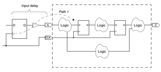
接下来将要分析的是被虚线框框住的设计。(将要)到达输入端口A的数据被CLK时钟驱动的外部时序器件发射。然后该数据在通过输入端口A前通过了一些组合逻辑电路。为了分析路径1的时序,你需要指定从时钟边沿到的数据到达输入端口A处的延迟大小。在这个例子中,输入延迟是外部触发器CLK-to-Q的延迟加上外部缓冲器的延迟。为了获得从输入端口A到设计中的组合逻辑之间的更精确的延迟计算结果,你也可以指定外部缓冲器的驱动特性。
The design being analyzed is enclosed in the dashed rectangle. The data arriving at input port "A" is launched by an external sequential device clocked by CLK. Then the data passes through some combinational logic before reaching input "A." To analyze the timing of Path 1,you need to specify the amount of delay from the clock edge to the arrival of data at input "A." In this example, the input delay is the CLK-to-Q delay of the external flip-flop plus the delay of the external buffer. You can also specify the drive characteristics of the external buffer for a more accurate calculation of the interconnect delay from input "A" to the combinational logic inside the design.
同样地,对于一个在设计输出端结束的路径,不能从设计的网表中确定数据的捕获时间。这是因为捕获时间和外部逻辑延迟是未知的。因此,要分析寄存器到输出的时间安排,必须指定外部定时条件超出了输出作为输出延迟。这个概念在图1-11中进行了阐释。
Similarly, for a path ending at an output of the design, the capture time of the data cannot be determined from the design netlist. This is because the capture time and external logic delays are unknown. Therefore, to analyze the register-to-output timing, you must specify the external timing conditions beyond the output as an output delay. This concept is illustrated in Figure 1-11.
图1-11 外部输出延迟
Figure 1-11 External Output Delay

从输出端口Z离开的数据经过了一些组合逻辑电路并被CLK时钟驱动的外部时序元件捕获。为了分析路径3的时序,你需要指定从输出端Z的到达的数据到捕获时钟边沿的延迟大小。在这个例子中,输出延时是外部缓冲器的延时加上外部触发器的建立时间要求,你应该指定外部电路的负载特性来精确计算到输出端Z的内部互连线的延迟。指定输入延迟和输出延迟的命令是set_input_delay与set_output_delay.
The data leaving output port "Z" passes through some combinational logic and is captured by an external sequential device clocked by CLK. To analyze the timing of Path 3, you need to specify the amount of delay from the arrival of data at output "Z" to the capture clock edge. In this example, the output delay is the delay of the external buffer plus the setup time requirement for the external flip-flop. You should also specify the load characteristics of the external circuit to accurately account for the interconnect delay at the output "Z"The commands for specifying input delays and output delays are set_input_delay and set_output_delay.