Introduction to Synthesis Timing(1)
RTL综合时序介绍(1)
Static timing analysis is a method of validating the timing performance of a design bychecking all possible paths for timing violations under worst-case conditions. It considers the worst possible delay through each logic element, but not the logical operation of the circuit.
静态时序分析是一种通过检查在最坏情况下所有可能存在时序违例的路径来验证设计的时序性能的方法。它考虑了每个逻辑单元的最差延迟,而不是考虑电路的逻辑操作。
In comparison to circuit simulation, static timing analysis is faster and more thorough. It is faster because it does not need to simulate multiple test vectors.
相对于电路仿真而言,静态时序分析更快也更深入。因为它不需要模拟多个仿真向量,所以它更快。
It is more thorough because it checks the worst-case timing for all possible logic conditions, not just those sensitized by a particular set of test vectors.
它更深入,因为它检查了在所有可能得逻辑情况下的最差时间,而不是只对特定的一组测试向量敏感。
However, static timing analysis checks the design only for proper timing, not for correct logical functionality. Timing, area, and power constraints drive the operation of synthesis with Design Compiler and physical implementation with IC Compiler.
然而,静态时序分析只检查设计设计是否拥有合适的时序,而不会检查设计的逻辑正确性。时序,面积,功耗约束驱动着DC的综合操作与ICC的物理实现。
These tools synthesize the netlist and perform physical placement and routing with the goal of making the fastest device, using the least area and power, in the shortest turn around time that is consistent with the designrequirements.
这些工具综合了网表,并执行物理布局和布线,在最短的翻转时间内使用最少的面积和功耗,实现最快器件的目标,尽可能实现与设计目标一致的结果
These tools perform trade-offs between speed, area, power, and runtime according to the constraints set by the designer. However, a chip must meet the timing constraints to operate at the intended clock rate, so timing is the most important designconstraint.
这些工具需要根据设计者设置的约束在速度,面积,功耗,运行时间之间做出权衡取舍。然而,一块芯片必须要满足在预定时钟频率下的时序约束,所以时序是最重要的设计约束。
Static timing analysis seeks to answer the question, "Will the correct data be present at the data input of each synchronous device when the clock edge arrives, under all possible conditions?"
静态时序分析看起来是要在寻找这个问题的答案,即:在所有可能的情况下,当时钟沿到达时,正确的数据是否会及时出现在每个同步器件的数据出入端?
Figure 1-1 TIMING PATH
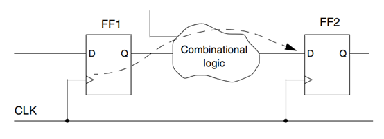
the dashed arrow represents a timing path. The change in signal data caused by a clock transition at flip-flop FF1 must be propagated to flip-flop FF2 before the following clock edge arrives at FF2, so that the logically processed data can be reliably latched into FF2. The change at FF1.Q might affect the output of the combinational logic cloud at FF2.D, depending on the logic itself, the data value, and the values of any side inputs feeding into the logic. The change at FF2.D, if any, must occur before the next clock edge arriving at FF2.
虚线箭头表示了一个时间路径,由于触发器FF1中的时钟转换导致的信号数据的改变必须在FF2的时钟上升沿之前到达,使得这个经过逻辑处理的数据可以被可靠的锁存进FF2。FF1_Q端的变化可能影响到在FF2_D端的组合逻辑块的输出,这取决于逻辑块的本身,数据的值,以及任何输入进逻辑块的值。FF2_D端的变化必须发生在FF2时钟边沿到达之前。
Figure 1-2 Setup Check Timing
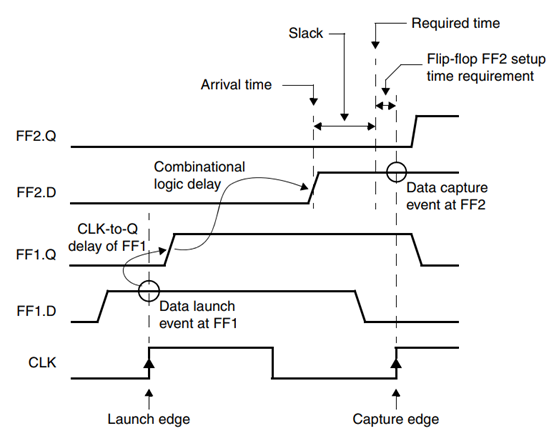
Figure 1-2 shows the timing for this path. The arrival of a clock edge at FF1 latches the data at the input FF1.D into the flip-flop. It also places that data on the flip-flop output, FF1.Q,after the clock-to-Q delay of the flip-flop. This is called the launch event for the timing path。
图1-2显示了这条路径的时序。当时钟边缘到达FF1时,FF1锁存FF1.D端的数据进入触发器。在经过触发器CLK to Q的延时过后,数据将放置在FF1.Q端。这个过程称为这条时钟路径的启动事件。
This signal goes through the combinational logic with some delay. The output of the
combinational logic is at the input of the second flip-flop, FF2.D. The time at which the signal value changes here is called the arrival time for the path.
这个信号穿过组合逻辑时会经过一些延时。组合逻辑的输出是第二个触发器FF2.D的输入。这里信号值变化的时间称为路径到达时间。
The change in value at FF2.D must occur before the arrival of the clock edge arriving at FF2,by at least an amount equal to the setup time requirement for the flip-flop. This latest allowable arrival time is called the required time for the path. The latching of data at FF2 is called the capture event for the timing path. In this example, the capture event occurs one whole clock cycle after the launch event.
FF2.D值变化必须在时钟边缘到达FF2之前发生,其发生时间至少等于触发器所需的建立时间。这个最小的允许到达时间称为路径的必需时间。FF2上的数据锁存称为时间路径的捕获事件。在本例中,捕获事件在启动事件之后的整个时钟周期内发生。`
The amount of time by which the timing constraint is met is called the slack of the timing check. If the signal arrives earlier than necessary as shown in Figure 1-2, the slack is positive. If the signal arrives exactly at the required time, the slack is zero and the timing constraint is barely met. If the signal arrives later than the required time, the slack is negative.
In all three cases, the amount of slack is the required time minus the arrival time.For example, if the required time is 1.8 ns after the launch clock edge and the arrival time is 1.6 ns after the launch clock edge, the slack is 1.8 minus 1.6, or 0.2 ns, a positive number.
满足时序约束的时间量称为时序检查的裕量。如图1-2所示,若信号提前到达,则裕量为正。如果信号恰好在要求的时间到达,则裕量为零,刚好满足时序约束。如果信号到达的比要求的满,那么裕量为负。在所有的三种情况中,裕量的大小等于所要求的时间减去实际到达的时间。比如在时钟沿触发后的要求时间为1.8ns,实际到达时间为时钟沿触发后1.6ns,那么时间裕量为0.2ns,为一个正值。
The preceding timing check is called a setup check, which verifies that a change in data arrives soon enough before each clock edge at the sequential device. This is the most common type of timing check that drives synthesis and optimization.
前面所述的时序检查称为建立(时间)检查,它验证数据的变化是否在时序设备的每个时钟边缘之前能够及时到达。这是用于综合和优化的最常见的时序检查类型。
However, other types of timing checks can be performed as well. For example, a hold check verifies that the data remains valid during and after the arrival of the clock edge at the end of the path by a sufficient amount.
A hold violation can occur if the shortest possible combinational delay from launch to capture is very short and the longest delay from the launch clock edge to the capture clock edge is very long. An example is shown in Figure 1-3 and Figure 1-4.
然而,还有一些其他类型的时序检查也需要执行。举例来说,一个保持(时间)检查验证在时间沿达到以及达到末端路径之后,数据是否保持一个足够的时间。当发射到捕获的最短可能的组合延迟非常短时,而从发射时钟到捕获时钟的最长延迟非常长时,可能会发生保持时间违例。
如图1-3和图1-4所示。
Figure 1-3 Hold Check Timing Path Example
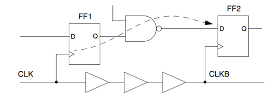
In Figure 1-3, the timing path has a very short combinational delay from FF1 to FF2,
consisting of a single NAND gate. Meanwhile, there is a long delay for the clock signal between the two flip-flops because of the three buffers, possibly made even longer by a large RC delay due to a long route. Therefore, the capture clock signal CLK2 arriving at FF2 is significantly delayed with respect to the launch clock CLK1 at FF1.
如图1-3所示,FF1到FF2的时序路径之间存在着很短的组合逻辑延迟,仅仅是一个与非门。同时,由于时钟路径上存在3个缓冲器,在两个触发器之间存在着一个很长的延时,甚至由于长路径导致的大的RC延迟,两者之间的延迟可能还会变的更大。
因此,捕获时钟信号CLK2到达FF2时显著落后于CLK1达到FF1的时间点。
Figure 1-4 Hold Check Timing

Figure 1-4 shows the possible timing in this situation. The setup constraint is met easily because the data arrives well before the required setup time. However, the hold constraint is not met because the data at the D input of FF2 is not held long enough after the nominal clock arrival time.
图1-4显示了这种情况下可能的时序。建立时间约束更容易满足,因为数据在需求的建立时间之前已经达到了。然而,保持时间约束不那么好满足,因为FF2输入端D上的数据输入在标准达到时间之后没有保持足够长的时间。
The data changes before the delayed clock CLK2 has a chance to latch it in. This type of violation can be fixed by shortening the delay in the clock line or by increasing the delay in the data path.
数据在已被延迟的时钟CLK2能够锁存他之前已经改变了。这种违例可以通过减少时钟线上的延迟或者通过增加数据通路上的延迟进行解决。
By default, the synthesis or implementation tool fixes setup violations, but not hold violations,because setup requirements are more difficult to satisfy.
默认情况下,综合或实现工具可以修复建立时间问题,但保持违例更难修复。
To have the tool fix hold violations as well as setup violations, use the set_fix_hold command.
如需工具在修复保持时间违例的同时修复建立时间违例,使用set_fix_hold命令
This command sets the fix_hold attribute on specified clocks, which directs the tool to check for and fix hold violations during the compile operation.
这个命令给特定的模块设定了fix_hold属性,该属性告诉工具在编译操作期间检查并修复保持时间违例。
Each type of timing check considers different worst-case conditions. For example, a setup check considers the longest and slowest possible path through the combinational logic of the data path and the earliest possible arrival of the capture clock edge with respect to the launch clock edge.
每种类型的时序检查考虑不同的最坏情况。举例来说,一个建立时间检查需要考虑通过组合逻辑的数据通路中最长和最短的可能路径,以及相对于发射时钟沿,捕获时钟沿最早可能到达的路径。
Conversely, a hold check considers the shortest and fastest possible path through the combinational logic of the data path and the latest possible arrival of the capture clock edge with respect to the launch clock edge.
相反的,一个保持时间检查需要考虑最短和最快的通过组合逻辑的可能的数据路径,以及相对于发射时钟沿最慢的捕获时钟沿的路径。
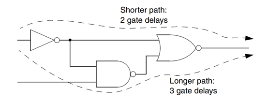
Figure 1-5 shows examples of different pathways that can be taken through the same block of combinational logic. In a data path, a setup check would consider the longer delay through three gates, whereas a hold check would consider the shorter path through two gates.
图1-5 显示了通过同样一个组合逻辑块不同的路径。在一个数据路径中,建立时间检查需要考虑通过三个门的更长的延时,而保持时间检查将考虑通过两个门的更短的延时。
A synthesis, optimization, or analysis tool can perform timing checks on the following types of paths:
一个综合、优化或者分析工具可以对以下种类的路径执行时序检查:
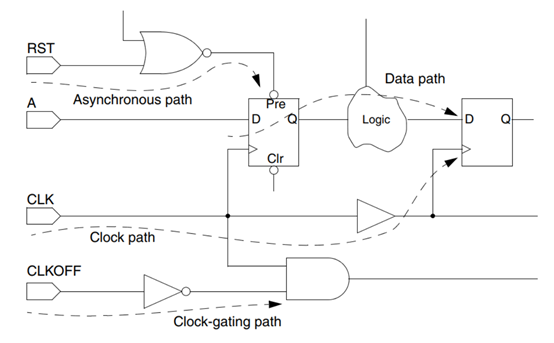
• Clock path (a path from a clock input port or cell pin, through one or more buffers or inverters, to the clock pin of a sequential element) for data setup and hold checks
时钟路径(从时钟输入端口或单元管脚,通过一个或多个缓冲器或反相器,到时序元件的时钟管脚的一种路径)
• Clock-gating path (a path from an input port to a clock-gating element) for clock-gating setup and hold checks
•时钟门控路径(从输入端口到时钟门控单元的路径),用于设置时钟门控并进行检查
• Asynchronous path (a path from an input port to an asynchronous set or clear pin of a sequential element) for recovery and removal checks
用于恢复和清除检查的异步路径(从输入端口到时序单元的异步置位或清除引脚的路径)
• Data-to-data check (a custom timing check specified with the set_data_check command, having specified setup and hold times between data signals)
数据到数据路径检查(使用set_data_check命令指定的自定义时序检查,指定了数据信号之间的建立和保持时间)
Some of these path types are shown in Figure 1-6
Figure 1-6 Path Types
A tool can also perform timing checks on the asynchronous preset and clear inputs of sequential devices. A recovery check verifies that enough time has passed after the inactivation of an asynchronous control signal before a clock edge occurs.
工具还可以对输入时序单元的异步预置和清除信号执行时序检查。恢复检查验证在时钟沿到来之前,离异步控制信号失效已经经过了足够长的时间。
A removal check verifies that enough time has passed after a clock edge before the removal of an asynchronous control signal. These types of checking are enabled by setting the enable_recovery_removal_arcs variable to true.
清除检查会验证,在异步控制信号移除之前,离时钟沿已经经过了足够长的时间。
A clock-gating check is a setup or hold check performed on the control input of a clock-gating cell. This type of check detects occurrences of clipped clocked edges or spurious clock pulses. The command for specifying clock-gating checks is set_clock_gating_check.
时钟门控检查是一种对时钟门控单元的控制输入的建立时间和保持时间的检查。这种类型的检查检测削峰的时钟边沿或者虚假的时钟脉冲。这个用于指定时钟门控检查的命令是set_clock_gating_check