STA LEARN NOTE
- STA LEARN NOTE
- 基础知识部分
- 标准库单元及模型
- cell and library
- pin capacitance(引脚容值)
- timing model
- Threshold Specifications and Slew Derating(阈值域和slew系数)
- timing mode - combinational cell(时序模型-组合逻辑单元)
- timing mode-sequential cell(时序模型-时序单元)
- State-Dependent Models(状态相关模型)
- Interface Timing Model for a Black Box(黑盒接口时序模型)
- Advanced Timing Modeling(高级时序模型)
- Power Dissipation Modeling(功耗模型)
- delay calculation(延迟计算)
- configure STA environment
- BLOG SITE
Static Timing Analysis for Nanometer Designs: A Practical Approach
基础知识部分
transition delay(信号转换延迟)
transition delay指的是输入或输出端口信号H2L或L2H所需时间,
不是通过gate的时间
transition delay parameter(信号转换延迟相关参数)
PARAMETER MEANING slew_lower_threshold_pct_fall 下降沿,低位阈值电压百分比 slew_upper_threshold_pct_fall 下降沿,高位阈值电压百分比 slew_lower_threshold_pct_rise 上升沿,低位阈值电压百分比 slew_upper_threshold_pct_rise 上升沿,高位阈值电压百分比 fall/rise代表端口电平变化趋势,fall H2L,rise L2H
lower/upper代表变化趋势中的高位和低位,以百分比形式表达(10%90%)or(20%80%)
A slew rate is defined as a rate of change. In static timing analysis, the rising or falling waveforms are measured in terms of whether the transition is slow or fast. The slew is typically measured in terms of the transition time, that is, the time it takes for a signal to transition between two specific levels. Note that the transition time is actually inverse of the slew rate - the larger the transition time, the slower the slew, and vice versa.

slew rate定义为变化的速率。slew rate通常通过transition time计算,slew rate和transition time呈现出反比的关系,即transition time越大slew rate越小。
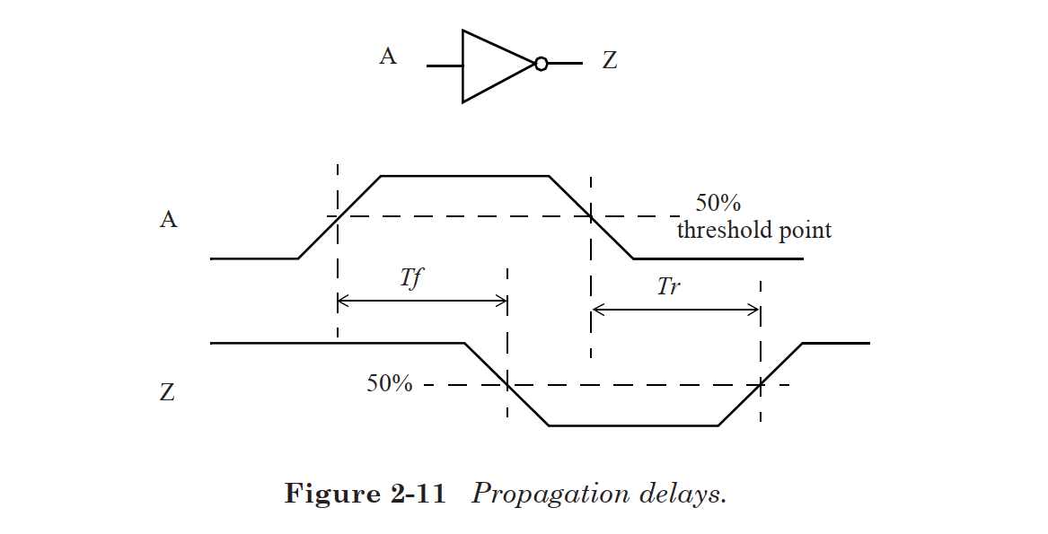
propagation delay(传播延迟)
propagation delay指的是输入信号50 percent VDD处时刻和输出端口信号50 percent VDD处的时间差
propagation delay parameter(逻辑门延迟相关参数)
PARAMETER MEANING input_threshold_pct_rise 输入端口上升沿百分比 output_threshold_pct_rise 输出端口上升沿百分比 input_threshold_pct_fall 输入端口下降沿百分比 output_threshold_pct_fall 输出端口下降沿百分比 fall/rise代表端口电平变化趋势,fall H2L,rise L2H
propagation delay百分比一般为50%
汉语表述部分是否是有问题的和英文中的定义不同
timing arc(时序弧)
1. positive unate timing arc(同向时序弧)
   A rising transition on an input causes the output to rise (or not to change) and a falling transition on an input causes the output to fall (or not to change).
2. negtive unate timing arc(反向时序弧)
   A rising transition on an input causes the output to have a falling transition (or not to change) and a fall-ing transition on an input causes the output to have a rising transition (or not to change).
3. non-unate timing arc(不定态时序弧)
   The output transition cannot be determined solely from the direction of change of an input but also depends upon the state of the other inputs.
setup/hold time(建立/保持时间)
建立时间:时序cell正常工作,保证功能正确,上升沿到来前数据保持稳定的最大时间
建立时间测量定义:数据信号电压到50 percent时刻与时钟信号电压达到50 percent时刻间的时间差(相较于std voltage)
The minimum time before the active clock when the data input must remain stable is called the
setup time.

This is measured as the time interval from the latest data signal crossing its threshold (normally 50% of Vdd) to the active clock edge crossing its threshold (normally 50% of Vdd).
保持时间:时序cell正常工作,保证功能正确,上升沿到来后数据保持稳定的最小时间
保持时间测量定义:时钟信号电压达到50 percent时刻与数据信号电压到50 percent时刻间的时间差(相较于std voltage)
the hold time is the minimum time the data input must remain stable just after the active edge of the clock. This is measured as the time interval from the active clock edge crossing its threshold to the earliest data signal crossing its threshold.
建立时间的分析是基于路径的最大延迟;而对于保持时间的分析是基于路径的最小延迟。
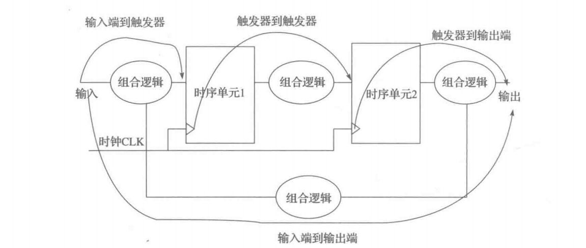
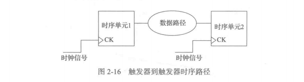
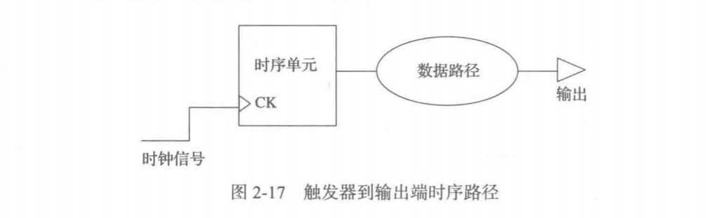
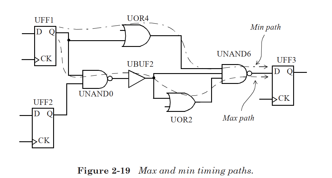
timing path(时序路径)
timing path指起点和终点间的path
start point::组合逻辑单元数据输入端口或时序单元clk输入端口
end point:组合逻辑单元数据输出端口或时序单元数据输入端口
TYPE MEANING input to output 组合逻辑单元数据输入端口到组合逻辑单元数据输出端口 input to register 组合逻辑单元数据输入端口到时序逻辑单元数据输入端口 register to output 时序逻辑单元时钟输入端口到组合逻辑单元数据输出端口 register to register 时序逻辑单元时钟输入端口到时序逻辑单元数据输入端口 from an input port to an output port from an input port to an input of a flip-flop or a memory, from the clock pin of a flip-flop or a memory to an input of flipflop or a memory, from the clock pin of a flip-flop to an output port
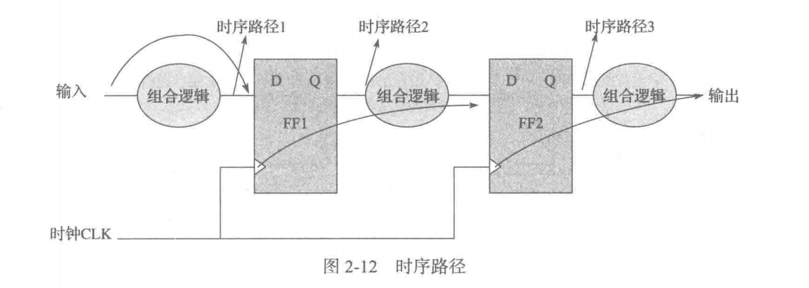
path delay:信号从start point经过某一路径到达endpoint的总时间称作路径延迟
max timing path(最大时序路径):The path from start point to endpoint need max timing called max timing path[ longest path ]
min timing path(最小时序路径):The path form start point to endpoint need min timing called min timing path[ shortest path ]
clock skew(时钟偏斜)
clock skew指两个或多个信号间的时间差值
时钟从时钟源出发在不同时刻到达目的端口,时刻最大与最小的差之就是clock skew
Skew is the difference in timing between two or more signals, maybe data,clock or both. For example, if a clock tree has 500 end points and has a skew of 50ps, it means that the difference in latency between the longest path and the shortest clock path is 50ps.
可以通过以下语句对clock skew进行约束:
set_clock_uncertainty 0.250 -setup [get_clocks BZCLK]
set_clock_uncertainty 0.100 -hold  [get_clocks BZCLK]
clock jitter(时钟抖动)
clock jitter指的是时钟沿抖动而形成的一个窗口
Every real clock source has a finite amount of jitter - a window within which a clock edge can occur. The clock period jitter is determined by the type of clock generator utilized. In reality, there are no ideal clocks, that is, all clocks have a finite amount of jitter and the clock period jitter should be included while specifying the clock uncertainty.

One can specify different clock uncertainties for setup checks and for hold checks. The hold checks do not require the clock jitter to be included in the uncertainty and thus a smaller value of clock uncertainty is generally specified for hold.

Q:设定clock uncertaity,为什么hold可以不考虑jitter产生的影响
Q:clock uncertainty如何影响setup和hold
clock latency
clock latency指时钟从时钟源到达end point的时间差值
set_clock_latency 2.0 [get_clocks USBCLK]
clock domain(时钟域)
一组由同一个时钟信号驱动的触发器,那么这组触发器就在同一个时钟域
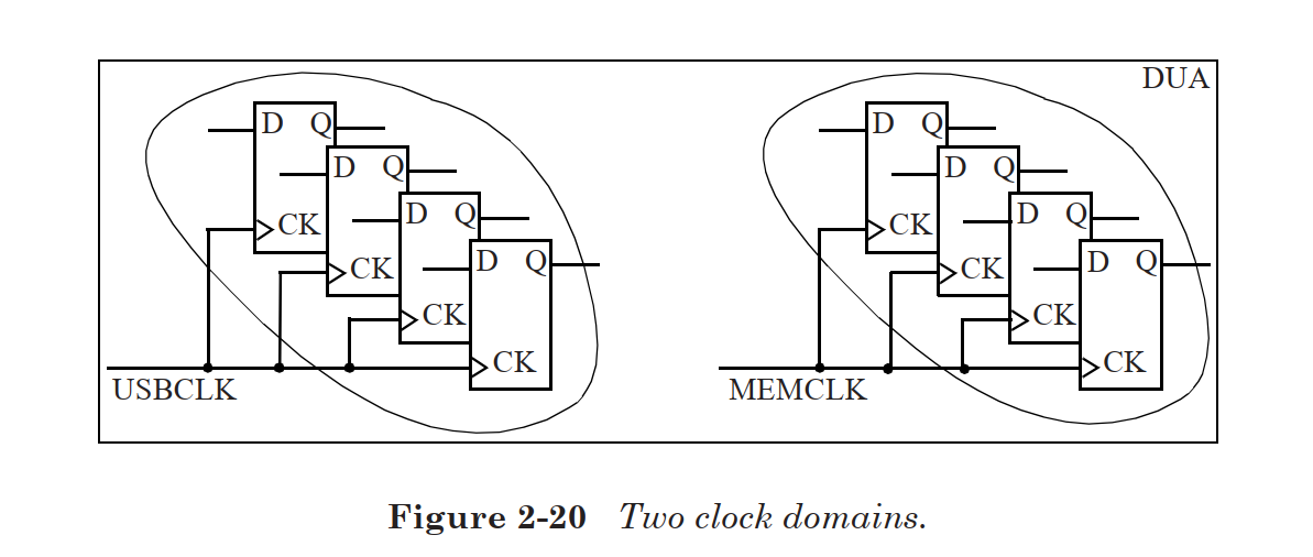
如何判断两个或多个时钟域之间是彼此独立或彼此相关的?
A:两时钟域是否相关取决于是否有data path从一个clock domain到另一个clock domain,如果没有则可以判定为时钟域相互独立。
A question of interest is whether the clock domains are related or independent of each other. The answer depends on whether there are any data paths that start from one clock domain and end in the other clock domain. If there are no such paths, we can safely say that the two clock domains are independent of each other. This means that there is no timing path that
starts from one clock domain and ends in the other clock domain.
如果时钟域彼此相关,如何判断data path是真还是假?
A:
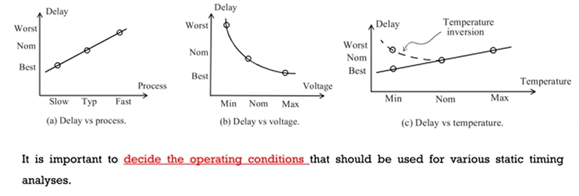
PVT operate conditions(PVT环境)
PVT可以分为typical,best,worst三种工艺环境
Item process voltage tempture TYP typical process nominal voltage nominal tempture BCF fast process highest voltage lowest tempture WCS slow process lowest voltage high to low TYP:typical
BCF:best case fast
WCS:worst case slow
WCS (Worst-Case Slow): Process is slow, temperature is highest(say 125C) and voltage is lowest (say nominal 1.2V minus 10%).For nanometer technologies that use low power supplies, there can be another worst-case slow corner that corresponds to the slow process, lowest power supply, and lowest temperature. The delays at low temperatures are not always smaller than the delays at higher temperatures.
在深纳米制程下,出现了温度反转现象,即在深纳米工艺下,温度越低,延迟越大
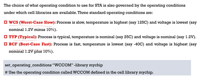
时序分析的同时还要考虑功耗,会加入另外两种工艺条件
ML(maximal leakage)极限功耗
TL(typical leakage)典型功耗
The environment conditions for power analysis are generally different than the ones used for static timing analysis. For power analysis, the operating conditions may be:

i. ML (Maximal Leakage): Process is fast, temperature is highest (say 125C) and the voltage is also the highest (say 1.2V plus 10%). This corner corresponds to the maximum leakage power. For most designs, this corner also corresponds to the largest active power.

ii. TL (Typical Leakage): Process is typical, temperature is highest(say 125C) and the voltage is nominal (say 1.2V). This refers to the condition where the leakage is representative for most designs since the chip temperature will be higher due to power dissipated in normal operation.
STA基于加载的库做运算分析:
set_operating_conditions “WCCOM” -library mychip
# Use the operating condition called WCCOM defined in the
# cell library mychip.
Item process voltage tempture ML fast process highest voltage highest tempture TL typical process nominal voltage nominal tempture
冷知识:
nom_process:工艺缩放因子(cell按照缩放比例扩大缩小?),缩放因子越小时序分析时延结果越小,缩放因子越大,时延结果越大。
tree_type:定义互连线延时计算模型(best_case_tree worst_case_tree balance_tree)
标准库单元及模型
cell and library
哪些可以被称作是cell?
A cell could be a standard cell, an IO buffer, or a complex IP such as a USB core and so on.library中包含哪些信息?
In addition to timing information, the library cell description contains several attributes such as cell area and functionality, which are unrelated to timing but are relevant during the RTL synthesis process.

library中包含除时序信息外还有cell的面积/功能这些与综合相关的信息。
pin capacitance(引脚容值)
每个cell都可以在其IO port上指定一个容值,但是多数情况下只对输入端口指定容值,所以在cell library中会看到输出引脚容值为0.
Every input and output of a cell can specify capacitance at the pin. In most cases, the capacitance is specified only for the cell inputs and not for the outputs, that is, the output pin capacitance in most cell libraries is 0.

pin (INP1) {
capacitance: 0.5;				    	    #most basic form
rise_capacitance: 0.5;				    	#rising transition pin capacitance
rise_capacitance_range: (0.48, 0.52);	 	 #rising transition pin capacitance range
fall_capacitance: 0.45;				    	#falling transition pin capacitance
fall_capacitance_range: (0.435, 0.46);        #falling transition pin capacitance range
. . .
}
timing model
The cell timing models are intended to provide accurate timing for various instances of the cell in the design environment. The timing models are normally obtained from detailed circuit simulations of the cell to model the actual scenario of the cell operation. The timing models are specified for each timing arc of the cell.

单元时序模型旨在为设计环境中的各种单元实例提供准确的时序。通常从单元的详细电路仿真中获得时序模型,以对单元操作的实际情况进行建模。为cell的每个时序弧指定timing model。
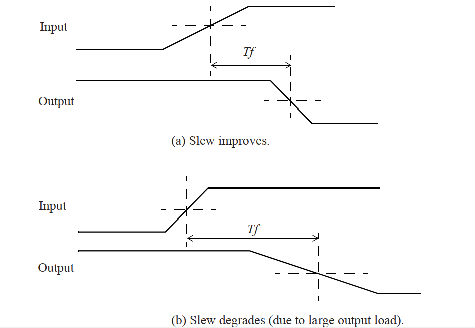
The delay values have a direct correlation with the load capacitance - the larger the load capacitance, the larger the delay. In most cases, the delay increases with increasing input transition time. There are a few scenarios where the input threshold (used for measuring delay) is significantly different from the internal switching point of the cell. In such cases, the delay through the cell may show non-monotonic behavior with respect to the input transition time - a larger input transition time may produce a smaller delay especially if the output is lightly loaded.

delay value和负载电容有直接的关系,负载电容值越大,delay也就越大(充放电时间长)。在大多数情况下,延迟随着输入转换时间的增加而增加。 在某些情况下,输入阈值(用于测量延迟)与单元的内部开关点明显不同。 在这种情况下,通过单元的延迟可能相对于输入转换时间表现出非单调行为-较大的输入转换时间可能会产生较小的延迟,尤其是在输出负载较轻的情况下。
linear delay model(线性延时模型)
线性时序模型中,cell delay和cell output transition time与input transition time和load capacitance呈现出线性关系。通常的表达形式为:
D = D0 + D1*s + D2*c
D				    #delay
s					#input transition time
c					#output load capacitance
D0/D1/D2			#constant value
这种线性时序模型在工艺进入亚微米时代不再适用
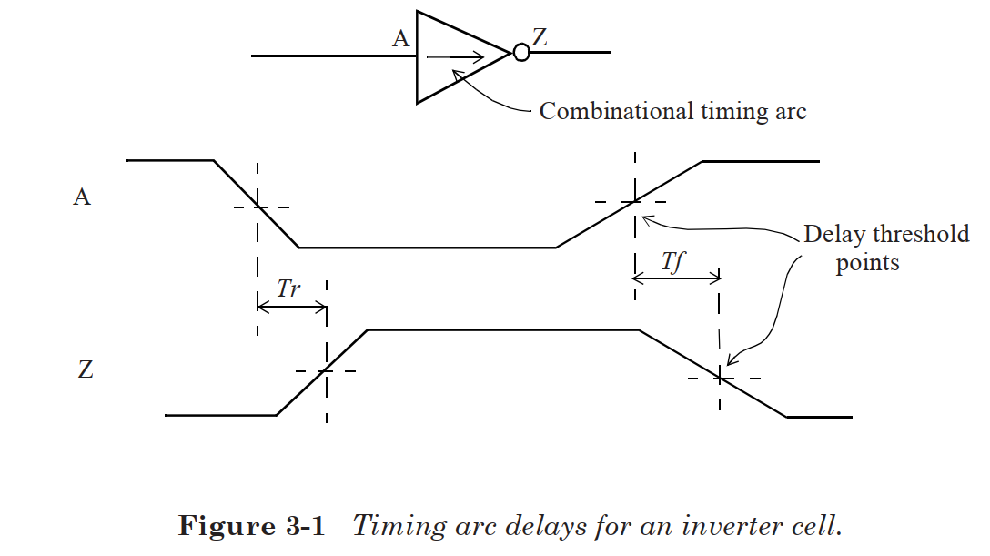
Tr:output rise delay
Tf:output fall delay
rise delay or fall delay通过测量input signal和其对应output signal 0.5倍VDD处时间差值进行测量(通常情况下是0.5倍VDD)
The delay for the timing arc through the inverter cell is dependent on two factors: the output load, that is, the capacitance load at the output pin of the inverter, and the transition time of the signal at the input.

反相器时序弧延迟主要取决于两个条件:输入端口信号transition time和输出端口负载电容值
输出端口信号slew rate主要取决于负载电容值,负载电容值越大output transition time也就越大。如上图所示就是通过调整output load capacitance调整output transition time。
non-linear delay model(非线性时序模型NLDM)
An NLDM model for delay is presented in a two-dimensional form, with the two independent variables being the input transition time and the output load capacitance, and the entries in the table denoting the delay.

非线性延时模型通过查找表的方式进行建模,索引值分别为input timing transition和output load capacitance。通过查找表找到对应的delay值和output transition time。
通过分析最简单的cell反相器的查找表理解非线性模型
pin (OUT) {
max_transition : 1.0;
timing() {
related_pin : "INP1";
timing_sense : negative_unate;
cell_rise(delay_template_3x3) {
index_1 ("0.1, 0.3, 0.7"); /* Input transition */
index_2 ("0.16, 0.35, 1.43"); /* Output capacitance */
values ( /* 0.16 0.35 1.43 */
/* 0.1 */ "0.0513, 0.1537, 0.5280",
/* 0.3 */ "0.1018, 0.2327, 0.6476",
/* 0.7 */ "0.1334, 0.2973, 0.7252");
}
cell_fall(delay_template_3x3) {
index_1 ("0.1, 0.3, 0.7"); /* Input transition */
index_2 ("0.16, 0.35, 1.43"); /* Output capacitance */
values ( /* 0.16 0.35 1.43 */
/* 0.1 */ "0.0617, 0.1537, 0.5280",
/* 0.3 */ "0.0918, 0.2027, 0.5676",
/* 0.7 */ "0.1034, 0.2273, 0.6452");
}
In the above example, the delays of the output pin OUT are described. This portion of the cell description contains the rising and falling delay models for the timing arc from pin INP1 to pin OUT, as well as the max_transition allowed time at pin OUT. There are separate models for the rise and fall delays (for the output pin) and these are labeled as cell_rise and cell_fall respectively.上表描述了反相器输出端口OUT查找表。查找表中定义了时序弧的信息,输出端口rise delay(max transition allowed at pin out)和fall delay(max transition allowed at pin out)在表中以cell_rise和cell_fall表示。cell_rise和cell_fall,fall和rise指的是输出端口信号变化趋势。查找表中定义的两个索引值分别为input transition time和output load capacitance,当知道这两个索引值后,就可以在value这一栏得知相应的delay值。
上表描述的是delay值
Example:假设一直input fall transition time为0.3,output load capacitance为0.1,应该如何通过查找表就行索引?
因为给的input transition time为fall时的值,所以输出端口信号变化为rise,所以应该在cell rise这一条目中索引,通过上表可得delay值为0.0513。
NLDM output transition time描述
The NLDM models are used not only for the delay but also for the transition time at the output of a cell which is characterized by the input transition time and the output load.
pin (OUT) {
max_transition : 1.0;
timing() {
related_pin : "INP";
timing_sense : negative_unate;
rise_transition(delay_template_3x3) {
index_1 ("0.1, 0.3, 0.7"); /* Input transition */
index_2 ("0.15, 0.35, 1.43"); /* Output capacitance */
values ( /* 0.15 0.35 1.43 */
/* 0.1 */ "0.0417, 0.1337, 0.4680",
/* 0.3 */ "0.0718, 0.1827, 0.5676",
/* 0.7 */ "0.1034, 0.2173, 0.6452");
} fall_transition(delay_template_3x3) {
index_1 ("0.1, 0.3, 0.7"); /* Input transition */
index_2 ("0.15, 0.35, 1.43"); /* Output capacitance */
values ( /* 0.15 0.35 1.43 */
/* 0.1 */ "0.0817, 0.1937, 0.7280",
/* 0.3 */ "0.1018, 0.2327, 0.7676",
/* 0.7 */ "0.1334, 0.2973, 0.8452");
}
通过NLDM delay look up table进行类比
Example:通常情况下,input transition time和output load capacitance在查找表找不到对应的值,假设假设input rising transition time为0.2,output load capacitance为0.25,output load capacitance为0.25,应该怎么处理?
input transition time x0 x1 x2 0.2 0.2 0.1 0.3
output load capacitance y0 y1 y2 0.25 0.25 0.15 0.35 所以计算(x0,y0)条件下delay或transition time:
If the table lookup is required for (x0, y0), the lookup value T00 is obtained by interpolation and is given by:
T00 = x20 * y20 * T11 + x20 * y01 * T12 + x01 * y20 * T21 + x01 * y01 * T22
where
x01 = (x0 - x1) / (x2 - x1) = 0.1 / 0.2 = 0.5
x20 = (x2 - x0) / (x2 - x1) = 0.1 / 0.2 = 0.5
y01 = (y0 - y1) / (y2 - y1) = 0.1 / 0.2 = 0.5
y20 = (y2 - y0) / (y2 - y1) = 0.1 / 0.2 = 0.5
T00 = 0.5 * 0.5 * 0.0817 + 0.5 * 0.5 * 0.1937 + 0.5 * 0.5 * 0.1018 + 0.5 * 0.5 * 0.2327 = 0.152475
还有一种情况就是input transition time和output load capacitance不在查找表的索引值范围内(0.1 ~0.3)/(0.15~1.43);假设input rising transition time = 0.05,output load capacitance = 1.7,应该怎么处理?
input transition time x0 x1 x2 0.05 0.05 0.1 0.3
output load capacitanc y0 y1 y2 1.7 1.70 0.35 1.43 T00 = x20 * y20 * T11 + x20 * y01 * T12 + x01 * y20 * T21 + x01 * y01 * T22 where x01 = (x0 - x1) / (x2 - x1) = -0.05 / 0.2 = -0.25 x20 = (x2 - x0) / (x2 - x1) = 0.25 / 0.2 = 1.25 y01 = (y0 - y1) / (y2 - y1) = 1.35 / 1.08 = 1.25 y20 = (y2 - y0) / (y2 - y1) = -0.27 / 1.08 = -0.25 T00 = 1.25 * -0.25 * 0.1937 + 1.25 * 1.21 * 0.7280 + -0.25 * -0.25 * 0.2327 + -0.25 * 1.25 * 0.7676 = -0.06053 + 1.1011 + 0.01454 - 0.23986 = 0.81525
inverter table 1 2 3 4 item cell rise cell fall rise transition fall transition
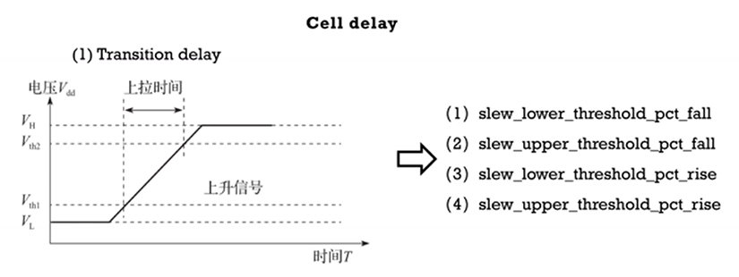
Threshold Specifications and Slew Derating(阈值域和slew系数)
As we all known,slew rate和transition time和阈值区间选取有关。在较早的工艺库中,通常指定阈值范围为VDD电压的(10~90 percent)测试slew。slew threshold的通常选择波形的线性部分。随着技术进步,波形线性部分更趋近于落在(30~70 percent)范围,所以新的时序库也将slew threshold指定在30~70 percent。但是通常测试的transition time通常在(10~90 percent),所以在(30~70 percent)测得的时间值仅有(10~90 percent)的1/2。所以在slew threshold指定为(30~70 percent)的库中会引入slew derate(0.5),以等效(10~90 percent)的测量值。
为什么引入slew derate?
A:因为slew measure threshold区间为(30~70 percent),而transition time measure thershold为(10~90 percent),所以引入slew derate,以使不同阈值域的定义可以达到等效的效果。
Example
/* Threshold definitions */
slew_lower_threshold_pct_fall : 30.0;
slew_upper_threshold_pct_fall : 70.0;
slew_lower_threshold_pct_rise : 30.0;
slew_upper_threshold_pct_rise : 70.0;
input_threshold_pct_fall : 50.0;
input_threshold_pct_rise : 50.0;
output_threshold_pct_fall : 50.0;
output_threshold_pct_rise : 50.0;
slew_derate_from_library : 0.5;

The above settings specify that the transition times in the library tables have to be multiplied by 0.5 to obtain the transition times which correspond to the slew threshold (30-70) settings.This means that the values in the transition tables (as well as corresponding index values) are effectively 10-90 values.
transition time乘以slew derate以获得在(30~70 percent)阈值域内相应的transition time。也就是说transition table中的数值实际对应的是阈值域为(10~90 percent)的值。
Example
threshold define between (20~80 percent)
/* Threshold definitions 20/80/1 */
slew_lower_threshold_pct_fall : 20.0;
slew_upper_threshold_pct_fall : 80.0;
slew_lower_threshold_pct_rise : 20.0;
slew_upper_threshold_pct_rise : 80.0;
/* slew_derate_from_library not specified */
slew_derate_from_library not specified(默认为1),也就是说transition table中threshold也为(20~80 percent)
Example
Here is another example of slew threshold settings in a cell library.
slew_lower_threshold_pct_rise : 20.00;
slew_upper_threshold_pct_rise : 80.00;
slew_lower_threshold_pct_fall : 20.00;
slew_upper_threshold_pct_fall : 80.00;
slew_derate_from_library : 0.6;
In this case, the slew_derate_from_library is set to 0.6 and characterization slew trip points are specified as 20% and 80%. This implies that transition table data in the library corresponds to 0% to 100% ((80 - 20)/(100 - 0) = 0.6) extrapolated values. This is shown in Figure 3-5.
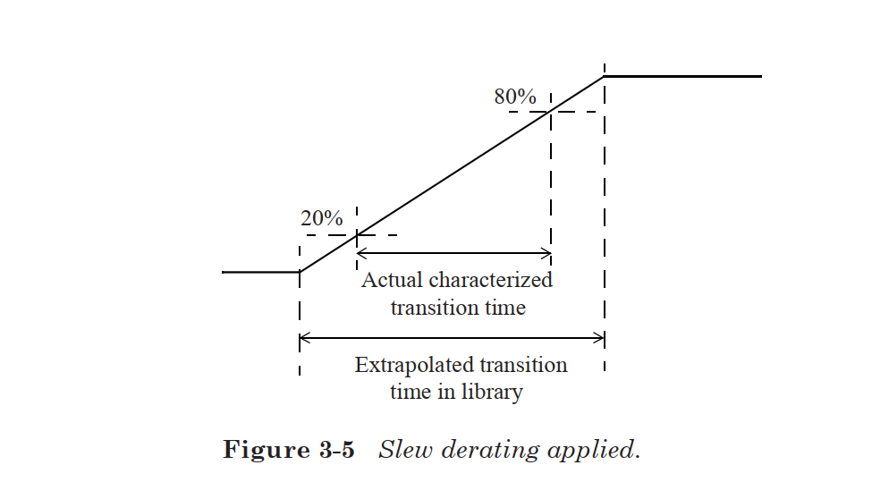
**When slew derating is specified, the slew value internally used during delay calculation is:
library_transition_time_value * slew_derate **
timing mode - combinational cell(时序模型-组合逻辑单元)
timing mode-sequential cell(时序模型-时序单元)
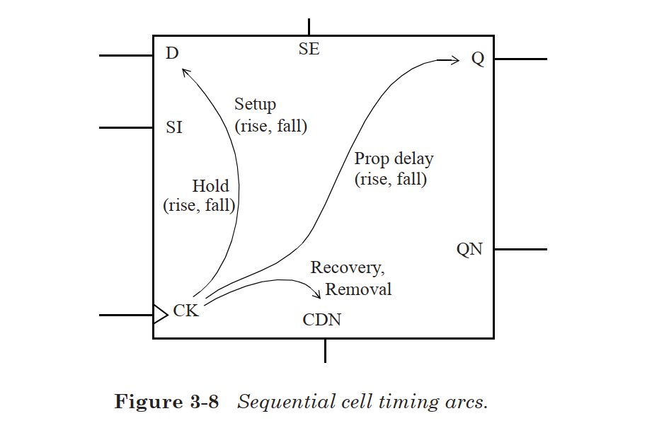
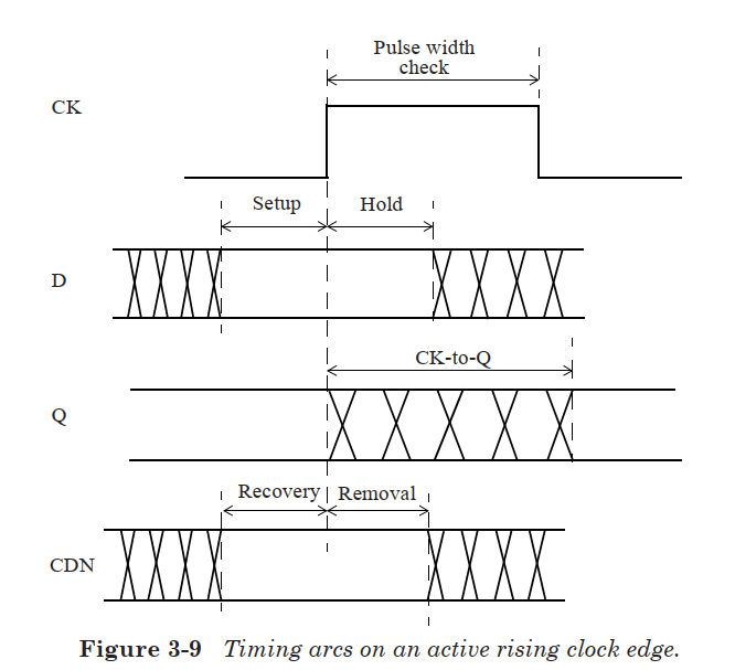
For synchronous inputs, such as pin D (or SI, SE), there are the following timing arcs:
i. Setup check arc (rising and falling)
ii. Hold check arc (rising and falling)

For asynchronous inputs, such as pin CDN, there are the following timing arcs:
i. Recovery check arc
ii. Removal check arc

For synchronous outputs of a flip-flop, such as pins Q or QN, there is the following timing arc:
i. CK-to-output propagation delay arc (rising and falling)
Synchronous Checks: Setup and Hold(同步时序:建立/保持检查)
setup/hold timing check和output slew/output transition time相似,也是以二位查找表的形式。output slew/output transition time相关的参数是input transition time and output load capacitance,setup和hold timing check相关参数为要检查的timing arc上start point和end point上的约束。
Example:
below shows the setup and hold timing information for the data pin of a flip-flop.
pin (D) {
direction : input;
. . .
timing () {
related_pin : "CK";
timing_type : "setup_rising";
rise_constraint ("setuphold_template_3x3") {
index_1("0.4, 0.57, 0.84"); /* Data transition */
index_2("0.4, 0.57, 0.84"); /* Clock transition */
values( /* 0.4 0.57 0.84 */
/* 0.4 */ "0.063, 0.093, 0.112",
/* 0.57 */ "0.526, 0.644, 0.824",
/* 0.84 */ "0.720, 0.839, 0.930");
}
fall_constraint ("setuphold_template_3x3") {
index_1("0.4, 0.57, 0.84"); /* Data transition */
index_2("0.4, 0.57, 0.84"); /* Clock transition */
values( /* 0.4 0.57 0.84 */
/* 0.4 */ "0.762, 0.895, 0.969",
/* 0.57 */ "0.804, 0.952, 0.166",
/* 0.84 */ "0.159, 0.170, 0.245");
}
}
}
timing () {
related_pin : "CK";
timing_type : "hold_rising";
rise_constraint ("setuphold_template_3x3") {
index_1("0.4, 0.57, 0.84"); /* Data transition */
index_2("0.4, 0.57, 0.84"); /* Clock transition */
values( /* 0.4 0.57 0.84 */
/* 0.4 */ "-0.220, -0.339, -0.584",
/* 0.57 */ "-0.247, -0.381, -0.729",
/* 0.84 */ "-0.398, -0.516, -0.864");
}
fall_constraint ("setuphold_template_3x3") {
index_1("0.4, 0.57, 0.84"); /* Data transition */
index_2("0.4, 0.57, 0.84");/* Clock transition */
values( /* 0.4 0.57 0.84 */
/* 0.4 */ "-0.028, -0.397, -0.489",
/* 0.57 */ "-0.408, -0.527, -0.649",
/* 0.84 */ "-0.705, -0.839, -0.580");
}
}
lu_table_template(setuphold_template_3x3) { variable_1 : constrained_pin_transition; variable_2 : related_pin_transition; index_1 ("1000, 1001, 1002"); index_2 ("1000, 1001, 1002"); }做flip-flop data pin上的setup/hold时序分析,相关约束为data constraint和clock constarint。
with a D pin rise transition time of 0.4ns and CK pin rise transition time of 0.84ns, the setup constraint for the rising edge of the D pin is 0.112ns - the value is read from the rise_constraint table.Q:lookup table中的rise contraint和fall constraint是指D pin还是指clk pin?
Note that the rise_constraint and fall_constraint tables of the setup constraint refer to the constrained_pin. The clock transition used is determined by the timing_type which specifies whether the cell is rising edge-triggered or falling edge-triggered.rise_constraint and fall_constraint都是和constraint pin相关的;setup/hold rising或setup/hold fall都适合时钟触发边沿类型相关的
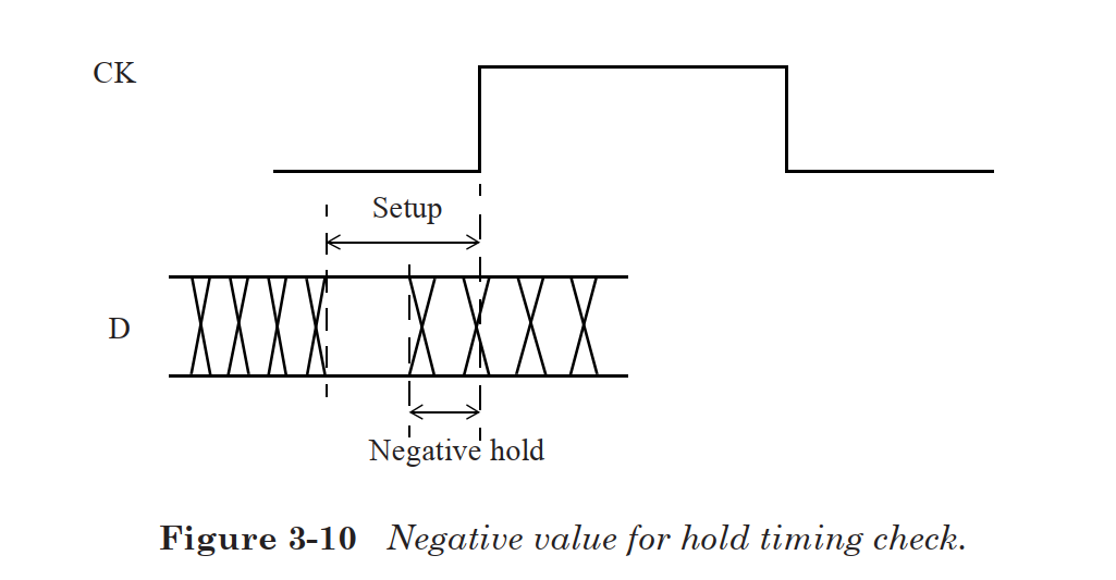
在hold timing check value中存在负数
This is acceptable and normally happens when the path from the pin of the flipflop to the internal latch point for the data is longer than the corresponding path for the clock. Thus, a negative hold check implies that the data pin of the flip-flop can change ahead of the clock pin and still meet the hold time check存在负数是正常的,当flip-flop pin到internal latch path要比clock path长时就会出现这种情况。当hold timing check为负数时就意味着ff引脚上的数据可以在时钟之前变化并始终满足hold timing check。
setup timing check value中是否会存在负数
The setup values of a flip-flop can also be negative. This means that at the pins of the flip-flop, the data can change after the clock pin and still meet the setup time check.setup timing check table中也可能会存在负数,负数意味着ff引脚上的数据可以在时钟之后改变并始终满足setup timing check。
setup/hold timing check value是否会都为负数
for the setup and hold checks to be consistent, the sum of setup and hold values should be positive. Thus, if the setup (or hold) check contains negative values - the corresponding hold (or setup) should be sufficiently positive so that the setup plus hold value is a positive quantity.答案是不会,hold value和setup value之和应该为正值,所以一个数值为负数另一个值必然为正数,不会出现两个值都为负的情况。
Since the setup has to occur prior to the hold, setup plus hold is a positive quantity. The setup plus hold time is the width of the region where the data signal is required to be steady.
hold check value为负数,所以setup check value为正数,且两者相加后的区域为数据应该稳定的时间段
Tips:
For flip-flops, it is helpful to have a negative hold time on scan data input pins. This gives flexibility in terms of clock skew and can eliminate the need for almost all buffer insertion for fixing hold violations in scan mode (scan mode is the one in which flip-flops are tied serially forming a scan chain - output of flip-flop is typically connected to the scan data input pin of the next flip-flop in series; these connections are for testability).
Asynchronous Checks (异步时序检查)
**Recovery and Removal Checks **(恢复/移除检查)
Asynchronous pins such as asynchronous clear or asynchronous set override any synchronous behavior of the cell. When an asynchronous pin is active, the output is governed by the asynchronous pin and not by the clock latching in the data inputs. However, when the asynchronous pin becomes inactive, the active edge of the clock starts latching in the data input. The asynchronous recovery and removal constraint checks verify that the asynchronous pin has returned unambiguously to an inactive state at the next active clock edge.异步信号有效时,cell正常的data到output pin会被打断。异步信号无效时,cell又会受到clock的控制将数据送达output端口。异步恢复/移除检查就是验证异步信号在下一个时钟有效沿前已经回到无效状态。
recovery time is the minimum time that an asynchronous input is stable after being de-asserted before the next active clock edge.恢复时间是指在下一个时钟沿有效前,异步输入引脚上的状态变为无效且保持稳定的最小时间。
removal time is the minimum time after an active clock edge that the asynchronous pin must remain active before it can be de-asserted移除时间是指在时钟有效沿之后,在异步输入引脚状态变为无效前,异步输入引脚上的状态需要保持有效的最小时间。
pulse width checks(脉宽检查)
脉宽要满足最小脉宽要求,否则可能导致cell不能正常的工作。除了可以对时钟引脚设定脉宽检查,也可以对同步或异步相关的引脚设定脉宽检查。
The minimumpulse width checks can be specified for high pulse and also for low pulse.
propagation delay(传播延迟)
The propagation delay of a sequential cell is from the active edge of the clock to a rising or falling edge on the output.
Example:
Here is an example of a propagation delay arc for a negative edge-triggered flip-flop, from clock pin CKN to output Q. This is a non-unate timing arc as the active edge of the clock can cause either a rising or a falling edge on the output Q. Here is the delay table:timing() { related_pin : "CKN"; timing_type : falling_edge; timing_sense : non_unate; cell_rise(delay_template_3x3) { index_1 ("0.1, 0.3, 0.7"); /* Clock transition */ index_2 ("0.16, 0.35, 1.43"); /* Output capacitance */ values ( /* 0.16 0.35 1.43 */ /* 0.1 */ "0.0513, 0.1537, 0.5280", /* 0.3 */ "0.1018, 0.2327, 0.6476", /* 0.7 */ "0.1334, 0.2973, 0.7252"); } rise_transition(delay_template_3x3) { index_1 ("0.1, 0.3, 0.7"); index_2 ("0.16, 0.35, 1.43"); values ( "0.0417, 0.1337, 0.4680", "0.0718, 0.1827, 0.5676", "0.1034, 0.2173, 0.6452"); } cell_fall(delay_template_3x3) { index_1 ("0.1, 0.3, 0.7"); index_2 ("0.16, 0.35, 1.43"); values ( "0.0617, 0.1537, 0.5280", "0.0918, 0.2027, 0.5676", "0.1034, 0.2273, 0.6452"); } fall_transition(delay_template_3x3) { index_1 ("0.1, 0.3, 0.7"); index_2 ("0.16, 0.35, 1.43"); values ( "0.0817, 0.1937, 0.7280", "0.1018, 0.2327, 0.7676", "0.1334, 0.2973, 0.8452"); } }flip-flop触发类型会由timing-type指定,因为cell是下降沿触发,所以要在fall transition中找input transition time。
State-Dependent Models(状态相关模型)
In many combinational blocks, the timing arcs between inputs and outputs depend on the state of other pins in the block. These timing arcs between input and output pins can be positive unate, negative unate, or both positive as well as negative unate arcs. An example is the xor or xnor cell where the timing to the output can be positive unate or negative unate. In such cases, the timing behaviors can be different depending upon the state of other inputs of the block. In general, multiple timing models depending upon the states of the pins are described. Such models are referred to as state-dependent models.
Interface Timing Model for a Black Box(黑盒接口时序模型)
The black box interface model can have combinational as well as sequential timing arcs. In general, these arcs can also be state-dependent.
a black box model can have the following timing arcs:

i. Input to output timing arcs for combinational logic paths.
ii. Setup and hold timing arcs from the synchronous inputs to the related clock pins.
iii. Recovery and removal timing arcs for the asynchronous inputs to the related clock pins.
iv. Output propagation delay from clock pins to the output pins.

The interface timing model as described above is not intended to capture the internal timing of the black box, but only the timing of its interfaces.
Advanced Timing Modeling(高级时序模型)
暂
Power Dissipation Modeling(功耗模型)
The cell library contains information related to power dissipation in the cells. This includes active power as well as standby or leakage power.

动态功耗 待机功耗 静态功耗
active power(动态功耗)
The active power is related to the activity at the input and output pin of the cell. The active power in the cell is due to charging of the output load as well as internal switching. These two are normally referred to as output switching power and internal switching power respectively.
output switching power
output switching power与cell类型无关,仅取决于输出负载电容大小/开关频率及power supply。
internal switching power
internal switching power(internal power)取决于cell type。
internal power library describe
pin (Z1) {
. . .
power_down_function : "!VDD + VSS";
related_power_pin : VDD;
related_ground_pin : VSS;
internal_power () {
related_pin : "A";
power (template_2x2) {
index_1 ("0.1, 0.4"); /* Input transition */
index_2 ("0.05, 0.1"); /* Output capacitance */
values ( /* 0.05 0.1 */
/* 0.1 */ "0.045, 0.050",
/* 0.4 */ "0.055, 0.056");
}
}
}

NOTE:因为表格中包含output capacitance,所以表格中的功耗仅对应于internal switching power,负载电容的功耗没有考虑在内。

The values represent the internal energy dissipated in the cell for each switching transition (rise or fall). The units are as derived from other units in the library (typically voltage is in volts (V) and capacitance is in picofarads (pF), and this maps to energy in picojoules (pJ)). The internal power in the library thus actually specifies the internal energy dissipated per transition.
leakage power(静态功耗)
暂
delay calculation(延迟计算)
delay calculation with interconnect(考虑互联寄生参数的延时计算)
pre-layout timing
post-layout timing
cell delay using effective capacitance(等效电容计算延时)
当考虑输出负载互联寄生电阻时,NLDM模型是不能直接使用的。所以采用有效电容的方法来解决寄生电阻对延时的影响。
the NLDM models are not directly usable when the load at the output of the cell includes the interconnect resistance. Instead, an “effective” capacitance approach is employed to handle the effect of resistance.等效电容的方法是通过一个电容等效原始负载,使得原始设计和等效后的设计时序表现相似。
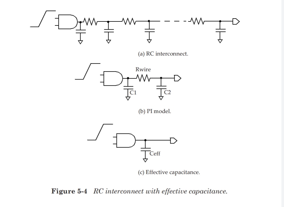
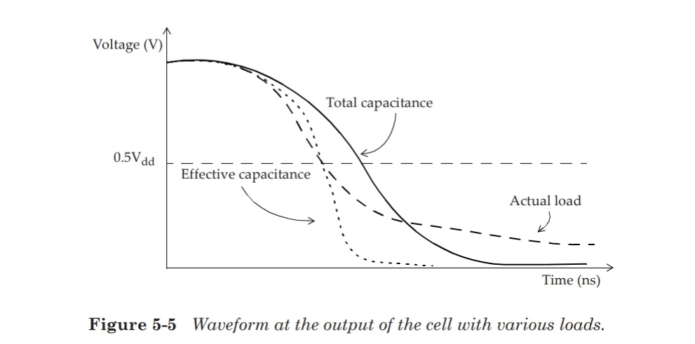
5-4(a) show a cell with an RC interconnect at its fanout
5-4(b) show an equivalent RC PI-network
5-4(c) show an equivalent output capacitance model
5-5 show output of the cell with total capacitance, effective capacitance and the waveform with the actual
RC interconnect.
等效电容计算:
In relation to the PI-equivalent representation, the effective capacitance can
be expressed as:

Ceff = C1 + k * C2, 0 <= k <= 1
C1是pi等效模型中的近端电容,C2是pi等效模型中的远端电容;当互联电阻值可以忽略不计时,等效电容值近似于总电容。当互联电阻值非常大时,等效电容值近似等于近端电容值(互联电阻值增加到无穷大)
slew merging
configure STA environment
specifying clocks
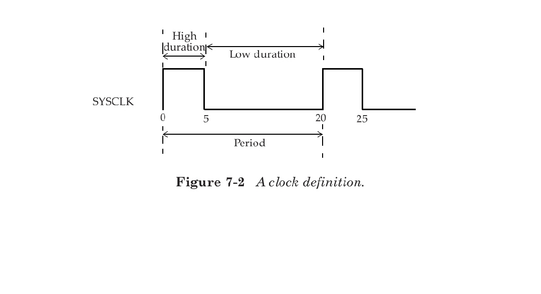
To define a clock,need these information
i. Clock source: it can be a port of the design, or be a pin of a cell inside the design (typically that is part of a clock generation logic).
ii. Period: the time period of the clock.
iii. Duty cycle: the high duration (positive phase) and the low duration (negative phase).
iv. Edge times: the times for the rising edge and the falling edge.

时钟源  周期  占空比  边沿时间
By defining the clocks, all the internal timing paths (all flip-flop to flip-flop paths) are constrained; this implies that all internal paths can be analyzed with just the clock specifications. The clock specification specifies that a flip-flop to flip-flop path must take one cycle. We shall later describe how this requirement (of one cycle timing) can be relaxed.

定义时钟后,内部时序路径都可以通过clock spec进行分析。clock spec指定了ff到ff路径仅只占用一个周期。
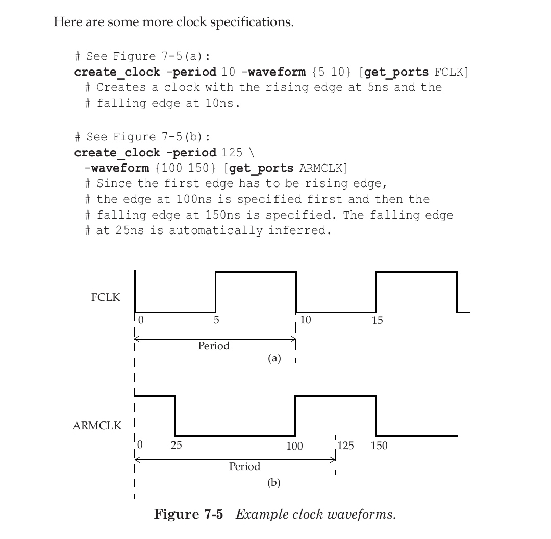
Here is a basic clock specification1.
create_clock
-name SYSCLK
-period 20
-waveform {0 5}
[get_ports SCLK]

The name of the clock is SYSCLK and is defined at the port SCLK. The period of SYSCLK is specified as 20 units - the default time unit is nanoseconds if none has been specified. (In general, the time unit is specified as part of the technology library.) The first argument in the waveform specifies the time at which rising edge occurs and the second argument specifies the time at which the falling edge occurs.
时钟名叫SYSCLK,SYSCLK被定义在SCLK,SYSCLK时钟周期为20个单位时间,0时刻上升沿5时刻下降沿。waveform选项中可以在时钟周期内指定任意多个边沿,上升沿下降沿依次交替。
waveform中边沿数量必须为偶数个,因为clock会重复waveform指定的过程。
如果没有设定waveform,默认为waveform {0, period/2};没有设定name,clock name会与get_ports一致。
In practice, it is a good idea to keep the clock name the same as the port name.
Example:
create_clock -name TEST_CLK -period 17 -waveform {0 8.5} -add [get_ports {ip_io_clk[0]}]
# The -add option allows more than one clock
# specification to be defined at a port.
除了在clock source上做上述设定外还可以为clock source指定transition time。例如PLL的输出,tool不能自动计算transition time,所以可以对clock source指定transition time。
set_clock_transition -rise 0.1 [get_clocks CLK_CONFIG]
set_clock_transition -fall 0.12 [get_clocks CLK_CONFIG]
set_clock_transition仅适用于理想时钟,构建时钟树后set_clock_transition将无效,将使用真实的transition time。
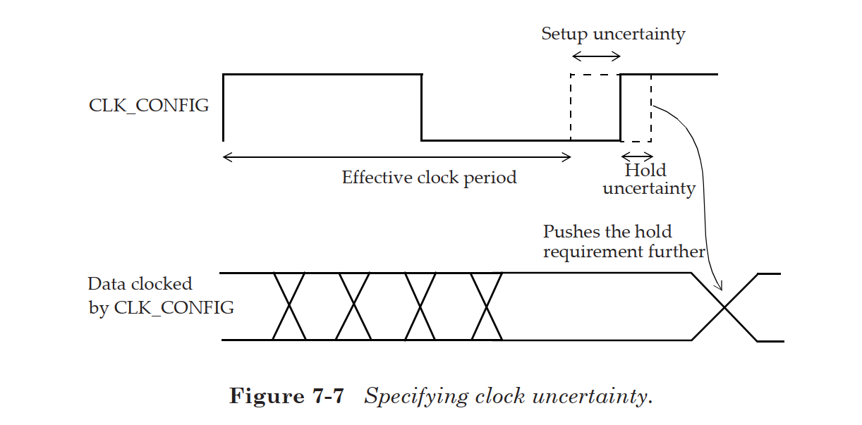
clock uncertainty(时钟不确定度)
The timing uncertainty of a clock period can be specified using the set_clock_uncertainty specification. The uncertainty can be used to model various factors that can reduce the effective clock period. These factors can be the clock jitter and any other pessimism that one may want to include for timing analysis.

时钟的那不确定度可以用set_clock_uncertainty指定。时钟不确定度设定模拟了各种影响时钟有效周期的一些因素,例如时钟抖动或其他因素。
set_clock_uncertainty -setup 0.2 [get_clocks CLK_CONFIG] set_clock_uncertainty -hold 0.05 [get_clocks CLK_CONFIG] Note that the clock uncertainty for setup effectively reduces the available clock period by the specified amount as illustrated in Figure 7-7. For hold checks, the clock uncertainty for hold is used as an additional timing margin that needs to be satisfied. 对setup设定的clock uncertainty,减少了可用的时钟周期。对hold设定的clock uncertainty,被用作需要满足时序的额外余量。
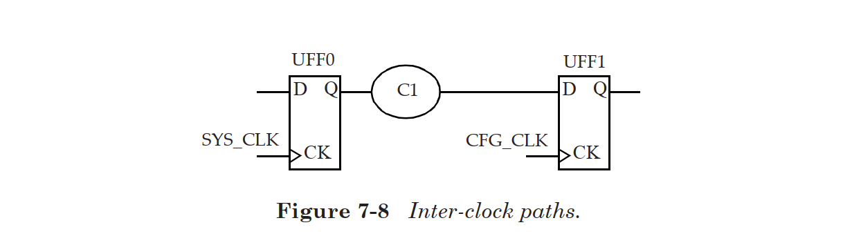
internal clock uncertainty
在跨时钟域系统可以通过下面command设定 clock uncertainty
set_clock_uncertainty -from SYS_CLK -to CFG_CLK -hold 0.05
set_clock_uncertainty -from SYS_CLK -to CFG_CLK -setup 0.1
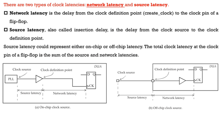
clock lantency
clock lantency有两种,一种是source lantency,另一种是network lantency.
source lantency(insertion delay)是从clock source到clock definition point点之间的延迟。
network lantency是从clock definition point到FF clock pin之间的延迟。
Total_Clock_Lantency=Source_Lantency+Network_Lantency
Network latency is the delay from the clock definition point (create_clock) to the clock pin of a flip-flop. Source latency, also called insertion delay, is the delay from the clock source to the clock definition point.The total clock latency at the clock pin of a flip-flop is the sum of the source and network latencies.Source latency could represent either on-chip or off-chip latency.
personal viewpoint:
source lantency之所以有片上和片外可能是因为芯片需要外部晶振提供基础时钟频率,再通过内部pll传送到definition point.
clock lantency command setting:
# Rise clock latency on MAIN_CLK is 1.8ns:
set_clock_latency 1.8 -rise [get_clocks MAIN_CLK]
# Fall clock latency on all clocks is 2.1ns:
set_clock_latency 2.1 -fall [all_clocks]
# The -rise, -fall refer to the edge at the clock pin of a
# flip-flop.
# Specify a network latency (no -source option) of 0.8ns for # rise, fall, max and min: set_clock_latency 0.8 [get_clocks CLK_CONFIG] # Specify a source latency: set_clock_latency 1.9 -source [get_clocks SYS_CLK] # Specify a min source latency: set_clock_latency 0.851 -source -min [get_clocks CFG_CLK] # Specify a max source latency: set_clock_latency 1.322 -source -max [get_clocks CFG_CLK]no -source option is network lantency
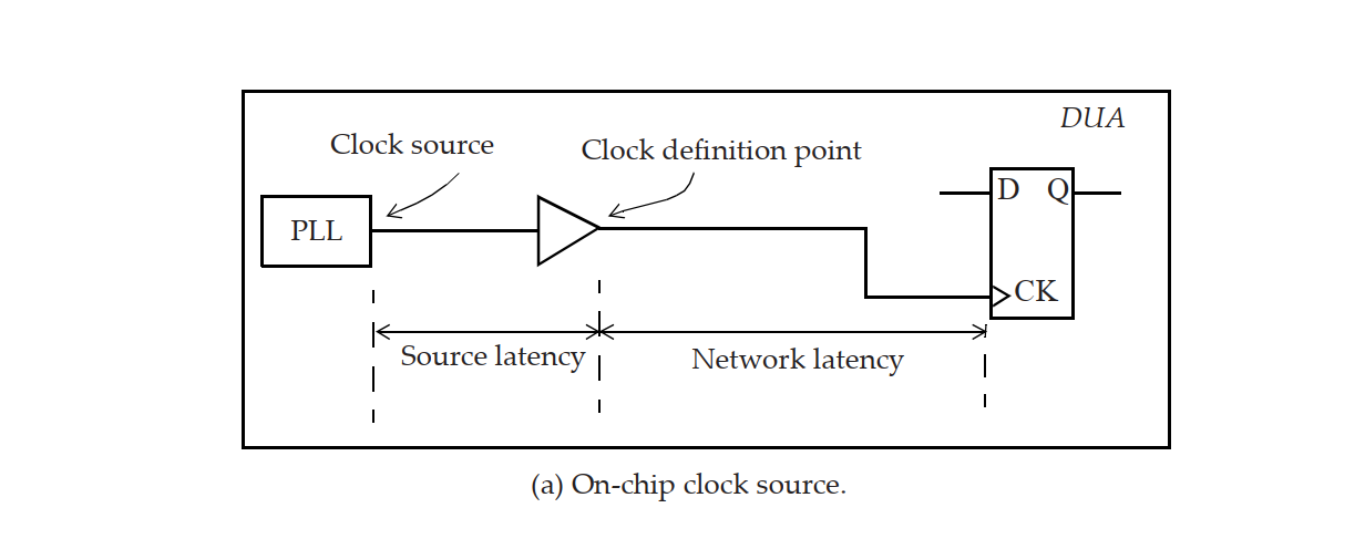
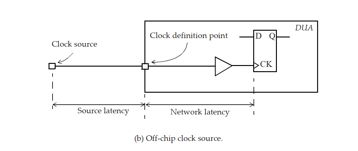
source lantency和network lantency最显著的区别
当系统的时钟树建立后,network lantency可以被忽略。即便时钟树已经建立但是source lantency依然存在。网络延迟是时钟树合成前对时钟树延迟的估计,时钟树综合后,从clock sorce到FF clk pin的时钟延迟等于source lantency + actual delay
One important distinction to observe between source and network latency is that once a clock tree is built for a design, the network latency can be ignored (assuming set_propagated_clock command is specified). However, the source latency remains even after the clock tree is built. The network latency is an estimate of the delay of the clock tree prior to clock tree synthesis. After clock tree synthesis, the total clock latency from clock source to a clock pin of a flip-flop is the source latency plus the actual delay of the clock tree from the clock definition point to the flip-flop.
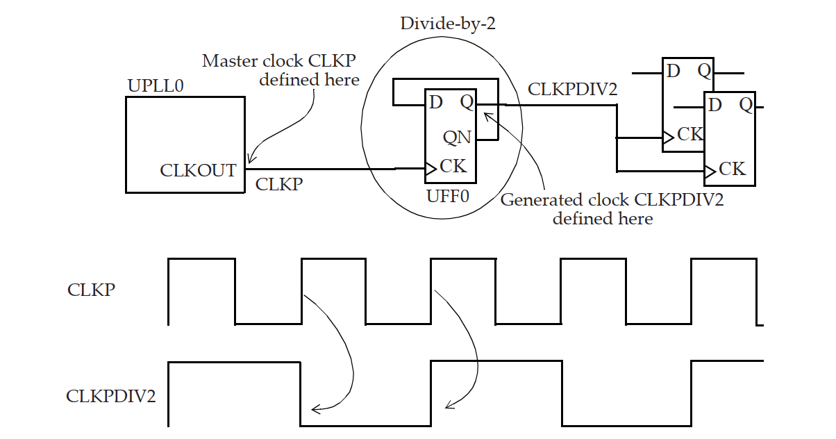
generate clock
generate clock是从master clock衍生出来的时钟,master clock是用create_clock规范定义的时钟。
A generated clock is a clock derived from a master clock. A master clock is a clock defined using the create_clock specification.基于主时钟定义generate clock时,需要知道generate clock的周期或者是分频系数。
When a new clock is generated in a design that is based on a master clock,the new clock can be defined as a generated clock. For example, if there is a divide-by-3 circuitry for a clock, one would define a generated clock definition at the output of this circuitry. This definition is needed as STA does not know that the clock period has changed at the output of the divide-by logic, and more importantly what the new clock period is.generate clock定义规范
create_clock -name CLKP 10 [get_pins UPLL0/CLKOUT]
# Create a master clock with name CLKP of period 10ns
# with 50% duty cycle at the CLKOUT pin of the PLL.
create_generated_clock -name CLKPDIV2 -source UPLL0/CLKOUT
-divide_by 2 [get_pins UFF0/Q]
# Creates a generated clock with name CLKPDIV2 at the Q
# pin of flip-flop UFF0. The master clock is at the CLKOUT
# pin of PLL. And the period of the generated clock is double
# that of the clock CLKP, that is, 20ns.
一个新衍生出来的时钟可以定义为master clock而不是用generate clock来定义吗?
答案是可以,但是会存在一些“问题”。除了多时钟域的情况下通常情况下也可以这样设定,当定义一个新clock为master clock后相当于新创建了一个clock domain。将新clcok定义为generate clock则不会创建了一个clock domain,generate clcok被认为是和master clock同相的,generate clock不需要一些额外的constraints。新的master clock的source lantency也不会包含在内。
master clock和generate clock还有一个显著区别就是clock origin的区别。master clock的clock origin是master clock的definition point,generate clock的clock origin是master clock。所以在clock path report中start point总是master clock的definition point。
Can a new clock, that is, a master clock, be defined at the output of the flipflop instead of a generated clock? The answer is yes, that it is indeed possible. However, there are some disadvantages. Defining a master clock instead of a generated clock creates a new clock domain. This is not a problem in general except that there are more clock domains to deal with in setting up the constraints for STA. Defining the new clock as a generated clock does not create a new clock domain, and the generated clock is considered to be in phase with its master clock. The generated clock does not require additional constraints to be developed. Thus, one must attempt to define a new internally generated clock as a generated clock instead of deciding to declare it as another master clock.

Another important difference between a master clock and a generated clock is the notion of clock origin. In a master clock, the origin of the clock is at the point of definition of the master clock. In a generated clock, the clock origin is that of the master clock and not that of the generated clock.This implies that in a clock path report, the start point of a clock path is always the master clock definition point. This is a big advantage of a generated clock over defining a new master clock as the source latency is not automatically included for the case of a new master clock.
两路时钟通过mux
多路复用器的输入端口为时钟信号,当在mux选择信号设定constraint,此时不需要在output定义一个时钟,输入输出信号具有相同属性。
如果没有在mux sel端设定constraint,时钟信号都会通过mux从而产生两路时钟信号间的sta report,但是这种情况是不可能发生的,因为sel端只能使一路时钟信号通过mux。所以在这种情况下需要设定false path或是指定两组时钟间的特定关系以避免生成错误的报告,(假定两组时钟信号间没有clock path)。
Figure 7-11 shows an example of a multiplexer with clocks on both its inputs. In this case, it is not necessary to define a clock on the output of the multiplexer. If the select signal is set to a constant, the output of the multiplexer automatically gets the correct clock propagated. If the select pin of the multiplexer is unconstrained, both the clocks propagate through the multiplexer for the purposes of the STA. In such cases, the STA may report paths between TCLK and TCLKDIV5. Note that such paths are not possible as the select line can select only one of the multiplexer inputs. In such a case, one may need to set a false path or specify an exclusive clock relationship between these two clocks to avoid incorrect paths being reported. This of course assumes that there are no paths between TCLK and TCLKDIV5 elsewhere in the design.
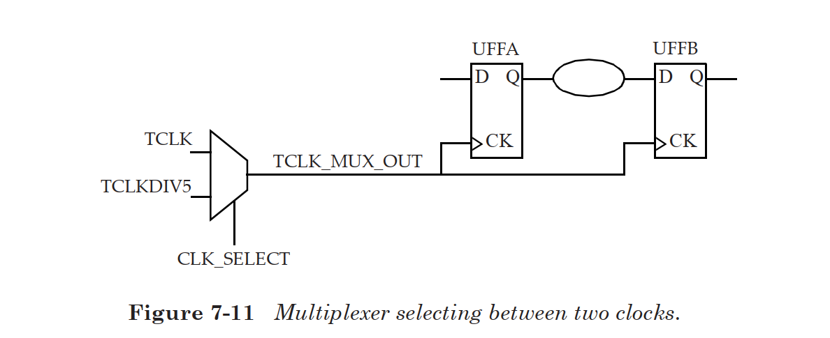
设备运行过程中mux sel是可变的应该怎么办?
In such cases, clock gating checks are inferred for the multiplexer inputs. Clock gating checks are explained in Chapter 10; these checks ensure that the clocks at the multiplexer inputs switch safely with respect to the multiplexer select signal.

在这种情况下,推断出多路复用器输入的时钟门控检查。第10章解释了时钟门控检查;这些检查确保多路复用器输入端的时钟与多路复用器选择信号安全切换。
create_clock 0.1 [get_ports SYS_CLK]
# Create a master clock of period 100ps with 50%
# duty cycle.
create_generated_clock -name CORE_CLK -divide_by 1
-source SYS_CLK [get_pins UAND1/Z]
# Create a generated clock called CORE_CLK at the
# output of the and cell and the clock waveform is
# same as that of the master clock.
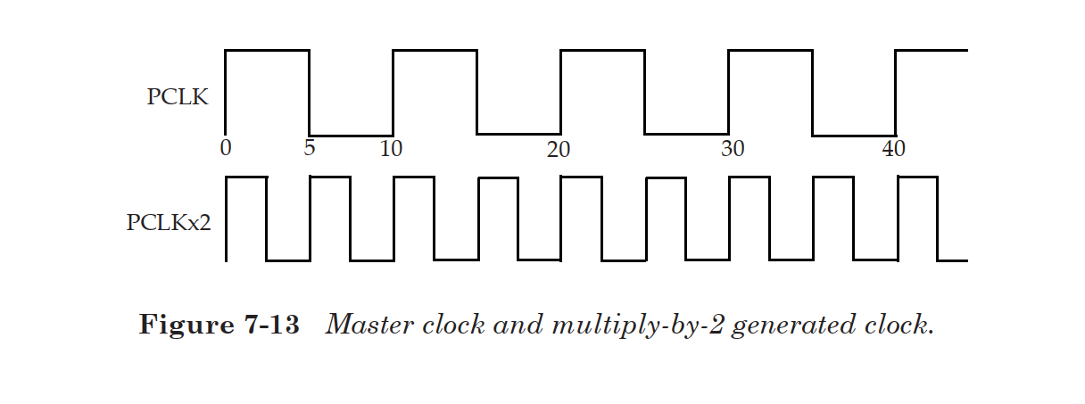
generate clock时钟频率高于master clock时钟频率
create_clock -period 10 -waveform {0 5} [get_ports PCLK]
# Create a master clock with name PCLK of period 10ns
# with rise edge at 0ns and fall edge at 5ns.
create_generated_clock -name PCLKx2
-source [get_ports PCLK]
-multiply_by 2 [get_pins UCLKMULTREG/Q]
# Creates a generated clock called PCLKx2 from the
# master clock PCLK and the frequency is double that of
# the master clock. The generated clock is defined at the
# output of the flip-flop UCLKMULTREG.
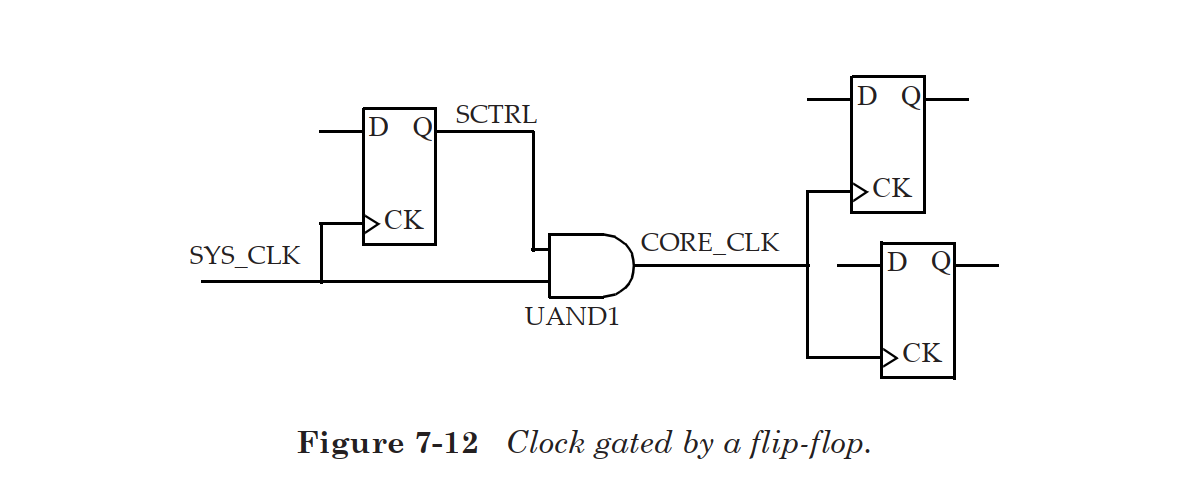
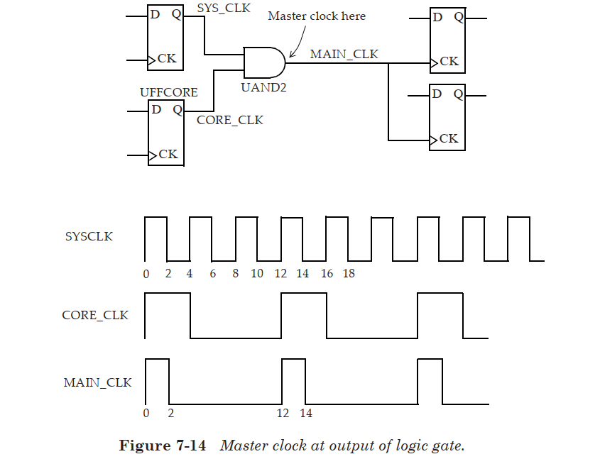
Master Clock at Clock Gating Cell Output
Consider the clock gating example shown in Figure 7-14. Two clocks are fed to an and cell. The question is what is at the output of the and cell. If the input to the and cell are both clocks, then it is safe to define a new main clock at the output of the and cell, since it is highly unlikely that the output of the cell has any phase relationship with either of the input clocks.

考虑图7-14所示的时钟门控例子。两个时钟被送入一个和单元。问题是在和单元的输出端是什么。如果和单元的输入都是时钟,那么在和单元的输出端定义一个新的主时钟是安全的,因为单元的输出与任何一个输入时钟都不太可能有任何相位关系。

One drawback of creating clocks at the internal pins is that it impacts the path delay computation and forces the designer to manually compute the source latencies.

在内部引脚处创建时钟的一个缺点是,它影响了路径延迟计算,迫使设计者手动计算源延迟。

create_clock -name SYS_CLK -period 4 -waveform {0 2}
[get_pins UFFSYS/Q]
create_clock -name CORE_CLK -period 12 -waveform {0 4}
[get_pins UFFCORE/Q]
create_clock -name MAIN_CLK -period 12 -waveform {0 2}
[get_pins UAND2/Z]
# Create a master clock instead of a generated clock
# at the output of the and cell.
generate clock with edge and edge_shift option
也可以通过-edge选项来定义一个generate clock,但是需要master clock以{rise,fall,rise}顺序的边沿列表来定义generate clock
The generated clock definition illustrates the -edges option, which is another way to define a generated clock. This option takes a list of edges {rise, fall, rise} of the source master clock to form the new generated clock.上图展示了DCLK经过二分频产生的时钟和两个相位不同的时钟信号,对这几个信号的定义如下所示:
create_clock 2 [get_ports DCLK]
# Name of clock is DCLK, has period of 2ns with a rise edge at 0ns and a fall edge at 1ns.

create_generated_clock -name DCLKDIV2 -edges {2 4 6} -source DCLK [get_pins UBUF2/Z]
# The generated clock with name DCLKDIV2 is defined at the output of the buffer. Its waveform is formed by having a rise edge at edge 2 of the source clock,fall edge at edge 4 of the source clock and the next rise edge at edge 6 of the source clock.

create_generated_clock -name PH0CLK -edges {3 4 7} -source DCLK [get_pins UAND0/Z]
# The generated clock PH0CLK is formed using the 3, 4, 7 edges of the source clock.

create_generated_clock -name PH1CLK -edges {1 2 5} -source DCLK [get_pins UAND1/Z]
# The generated clock with name PH1CLK is defined at the output of the and cell and is formed with edges 1, 2 and 5 of the source clock.
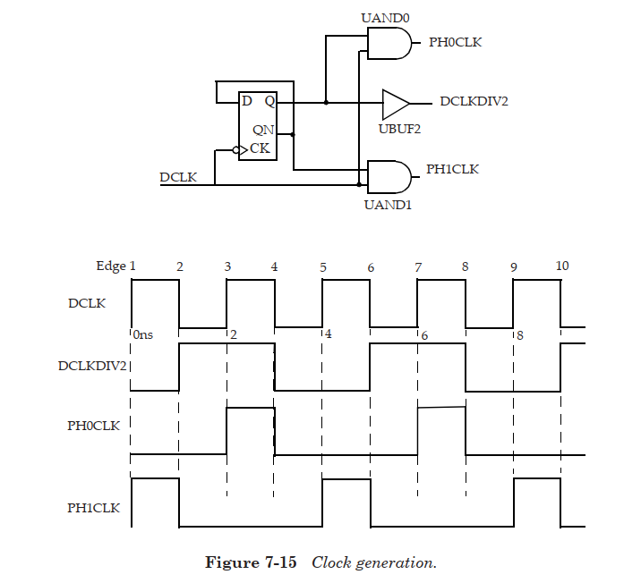
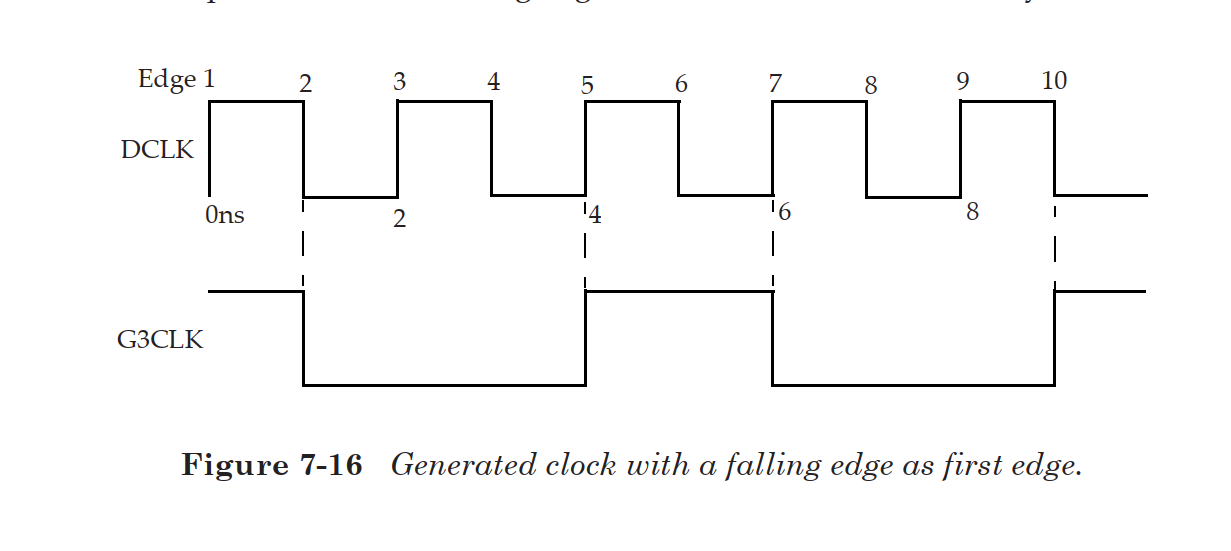
what if generate clock first edge is falling edge?
create_generated_clock -name G3CLK -edges {5 7 10} -source DCLK [get_pins UAND0/Z]如上定义方式会自动推断出1ns时刻为下降沿
edge选项可以和edge_shift选项联合使用定义新的generate clock,edge shift列表中定义了每个edge的偏移量
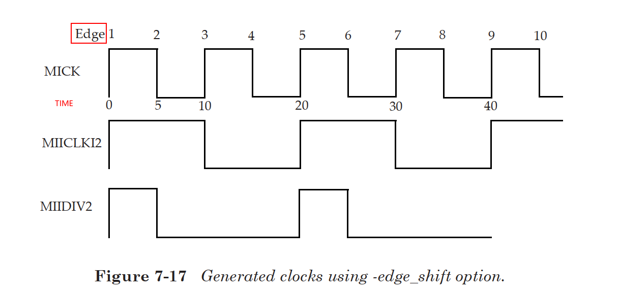
The -edge_shift option can be used in conjunction with the -edges option to specify any shift of the corresponding edges to form the new generated waveform. It specifies the amount of shift (in time units) for each edge in the edge list. Here is an example that uses this option.create_clock -period 10 -waveform {0 5} [get_ports MIICLK] create_generated_clock -name MIICLKDIV2 -source MIICLK -edges {1 3 5} [get_pins UMIICLKREG/Q] # Create a divide-by-2 clock. create_generated_clock -name MIIDIV2 -source MIICLK -edges {1 1 5} -edge_shift {0 5 0}[get_pins UMIIDIV/Q] # Creates a divide-by-2 clock with a duty cycle different from the source clock's value of 50%. #相较于source clock第一个边沿偏移0ns #相较于source clock第一个边沿偏移5ns #相较于source clock第五个边沿偏移0nsThe list of edges in the edge list must be in non-decreasing order, though the same edge can be used for two entries to indicate a clock pulse independent of the source clocks’ duty cycle. The -edge_shift option in the above example specifies that the first edge is obtained by shifting (edge 1 of source clock) by 0ns, the second edge is obtained by shifting (edge 1 of source clock) by 5ns and the third edge is obtained by shifting (edge 5 of source clock) by 0ns
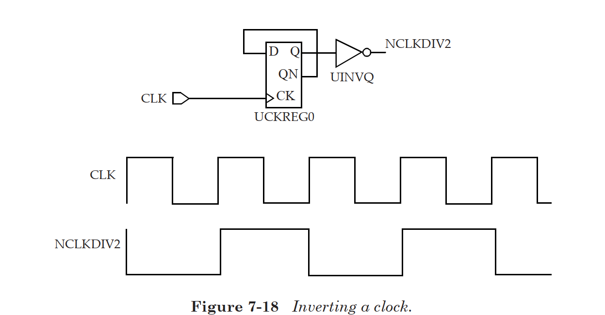
generate clock with invert option
generate clock其他所有选项生效后-invert选项才会起作用
create_clock -period 10 [get_ports CLK]

create_generated_clock -name NCLKDIV2 -divide_by 2 -invert -source CLK [get_pins UINVQ/Z]
The -invert option applies the inversion to the generated clock after all other generated clock options are applied.
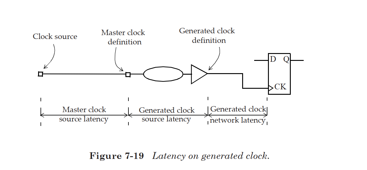
clock lantency for generate clock
generate clock也可以定义clock lantency. source lantency为master clock definition point到generate clock definition point点间的延迟;network lantency为generate clock definition point到FF clock pin.
Clock latencies can be specified for generated clocks as well. A source latency specified on a generated clock specifies the latency from the definition of the master clock to the definition of the generated clock. The total clock latency to a clock pin of a flop-flop being driven by a generated clock is thus the sum of the source latency of the master clock, the source latency of the generated clock and the network latency of the generated clock.
一个generate clock可以以另一个generate clock作为它的source clock,但是generate clock仅能有一个master clock
A generated clock can have another generated clock as its source, that is, one can have generated clocks of generated clocks, and so on. However, a generated clock can have only one master clock.
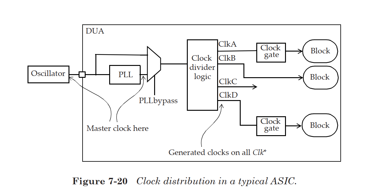
Typical Clock Generation Scenario
上图是典型的时钟拓扑方案,片外晶振为片内锁相环提供一个低频参考时钟,然后pll输出一个高频低抖动的时钟,再通过片内分频器为片内数字器件提供时钟信号。
时钟分支上可能还会有clock gate,用于关闭设计中不必要的时钟信号,降低功耗。也有可能在pll输出放置一个mux,在需要的时候可以bypass pll时钟信号。
On some of the branches of the clock distribution, there may be clock gates that are used to turn off the clock to an inactive portion of the design to save power when necessary. The PLL can also have a multiplexer at its output so that the PLL can be bypassed if necessary.第一个master clock定义在晶振信号输入引脚,第二个master clock定义在pll输出端。pll时钟信号和晶振时钟信号不存在相位关系,所以pll的输出时钟不应该定义为reference clock的generate clock。
A master clock is defined for the reference clock at the input pin of the chip where it enters the design, and a second master clock is defined at the output of the PLL. The PLL output clock has no phase relationship with the reference clock. Therefore, the output clock should not be a generated clock of the reference clock. Most likely, all clocks generated by the clock divider logic are specified as generated clocks of the master clock at the PLL output.
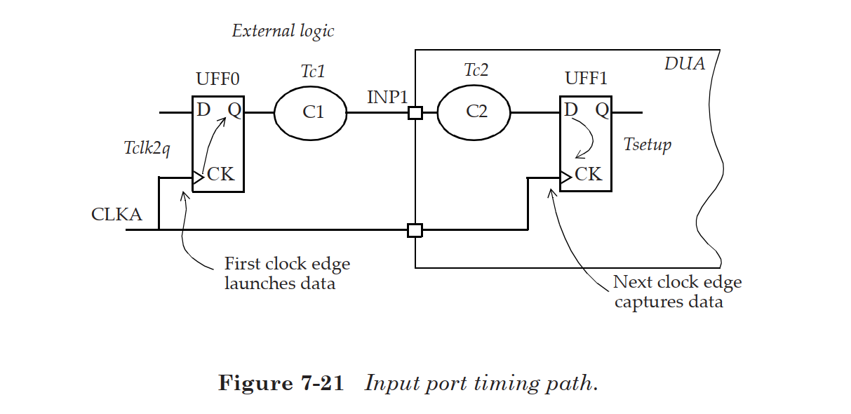
constraining input paths
STA不能对没有设定constarint的path做时序检查,除非有特殊需求不需要对某些path做时序检查不用设定constraint;
Figure 7-21 shows an input path of the design under analysis (DUA). Flipflop UFF0 is external to the design and provides data to the flip-flop UFF1 which is internal to the design. The data is connected through the input port INP1.The clock definition for CLKA specifies the clock period, which is the total amount of time available between the two flip-flops UFF0 and UFF1. The time taken by the external logic is Tclk2q, the CK to Q delay of the launch flip-flop UFF0, plus Tc1, the delay through the external combinational logic. Thus, the delay specification on an input pin INP1 defines an external delay of Tclk2q plus Tc1. This delay is specified with respect to a clock, CLKA in this example.input delay constraint
set Tclk2q 0.9
set Tc1 0.6
set_input_delay -clock CLKA -max [expr Tclk2q + Tc1] [get_ports INP1]
相对于CLKA,输入引脚INP1的外部延迟为1.5ns,如果时钟周期是2ns,对于INP1仅有500ps的时间将数据传到内部逻辑。对于内部而言,T_c2+T_setup_uff1必须要小于500ps,才能保证UFF1稳定的捕获到UFF0的数据,上述约束为最大input delay。
The constraint specifies that the external delay on input INP1 is 1.5ns and this is with respect to the clock CLKA. Assuming the clock period for CLKA is 2ns, then the logic for INP1 pin has only 500ps (= 2ns - 1.5ns) available for propagating internally in the design. This input delay specification maps into the input constraint that Tc2 plus Tsetup of UFF1 must be less than 500ps for the flip-flop UFF1 to reliably capture the data launched by flip-flop UFF0. Note that the external delay above is specified as a max quantity.
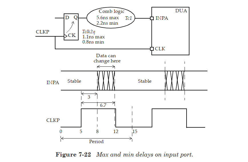
考虑input delay max/min这两种情况
做如下设定:
create_clock -period 15 -waveform {5 12} [get_ports CLKP]
set_input_delay -clock CLKP -max 6.7 [get_ports INPA]
set_input_delay -clock CLKP -min 3.0 [get_ports INPA]
input delay取决于从CLKP到INPA的延迟,min/max delay分别对应于min timing corner shortest path delay/max timing corner longest path delay.根据图中数据min input delay为3ns,max input delay为6.7ns。(相较于时钟信号有效沿)
在min timing corner,内部有效的setup time为15-3=12ns
在max timing corner,内部有效的setup time为15-6.7=8.3ns
所以内部捕获数据的有效时间为8.3ns
The max and min delays for INPA are derived from the CLKP to INPA delays. The max and min delays refer to the longest and shortest path delays respectively. These may also normally correspond to the worst-case slow (max timing corner) and the best-case fast (min timing corner). Thus, the max delay corresponds to the longest path delay at the max corner and the min delay corresponds to the shortest path delay at the min corner. In our example, 1.1ns and 0.8ns are the max and the min delay values for the Tck2q. The combinational path delay Tc1 has a max delay of 5.6ns and a min delay of 2.2ns. The waveform on INPA shows the window in which the data arrives at the design input and when it is expected to be stable. The max delay from CLKP to INPA is 6.7ns (= 1.1ns + 5.6ns). The min delay is 3ns (= 0.8ns + 2.2ns). These delays are specified with respect to the active edge of the clock. Given the external input delays, the available setup time internal to the design is the min of 8.3ns (= 15ns - 6.7ns) at the slow corner and 12ns (= 15ns - 3.0ns) at the fast corner. Thus, 8.3ns is the available time to reliably capture the data internal to the DUA.set_input_delay -clock clk_core 0.5 [get_ports bist_mode] set_input_delay -clock clk_core 0.5 [get_ports sad_state] 这种形式的约束,min/max input delay都为0.5ns上述的timing delay都是相较于时钟的上升沿,如果以时钟下降沿做参考可以指定-clock_fall选项
This external input delay is specified with respect to the rising edge of clock clk_core (the -clock_fall option has to be used if the input delay is specified with respect to the falling edge of the clock).
Constraining Output Paths
上图展示了一个输出端口的path,External_Logic_Total_delay=Tc2+Tsetup,the total delay is part of output delay.
输出延迟是相较于capture clock,数据必须及时到达UFF1数据端以满足setup要求。
set Tc2 3.9
set Tsetup 1.1
set_output_delay -clock CLKQ -max [expr Tc2 + Tsetup]
[get_ports OUTB]
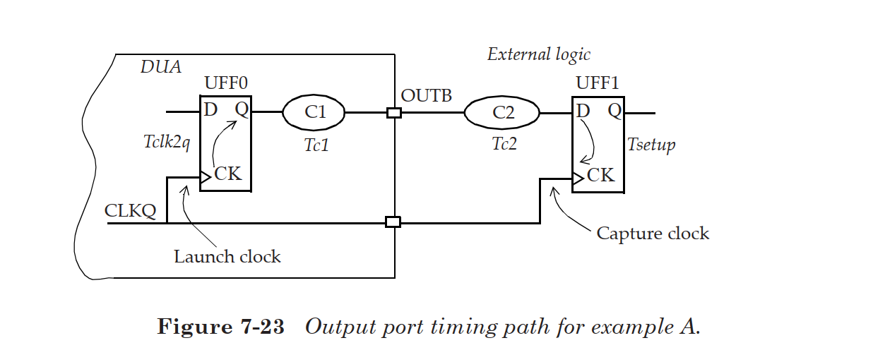
根据图示信息可以得到下述constraint:
create_clock -period 20 -waveform {0 15} [get_ports CLKQ]
set_output_delay -clock CLKQ -min -0.2 [get_ports OUTC]
set_output_delay -clock CLKQ -max 7.4 [get_ports OUTC]
min delay为负值,且使用hold time表示的
数据必须要按照要求在capture clock前后要求稳定的区域保持稳定,才能可靠的被capture clock捕获
create_clock -period 100 -waveform {5 55} [get_ports MCLK]
set_input_delay 25 -max -clock MCLK [get_ports DATAIN]
set_input_delay 5 -min -clock MCLK [get_ports DATAIN]
set_output_delay 20 -max -clock MCLK [get_ports DATAOUT]
set_output_delay -5 -min -clock MCLK [get_ports DATAOUT]
对于set input delay,数据可以发生变化的是constraint的交集区域
对于set output delay,数据必须要在constarint的并集区域保持稳定
Timing path group
设计中的timing path可以看作是路径的集合。
Timing paths in a design can be considered as a collection of paths.Timing path通过有效的startpoint和endpoint确定。
startpoint:input port or clk pin of sequential cell
endpoint:output port or data pin of sequential cell
summary of valid timing path
i. from an input port to an output port
ii. from an input port to an input of a flip-flop or a memory
iii. from the clock pin of a flip-flop or a memory to an input of flipflop or a memory
iv. from the clock pin of a flip-flop to an output port
v. from the clock pin of a memory to an output port
path group是根据路径endpoint相关的时钟来进行划分的,所以每个时钟都有其对应的path group,还有一个default path group用来将non_clocked path划分在一起
The static timing analysis and reporting are typically performed on each path group separately.
Modeling of External Attributes
drive strength
creat clock/set_in.output_delay/set_clock_lantency等虽然已经一些条件做了设定,但为了使模型更加精确还需要对IO pin外部属性做限制。
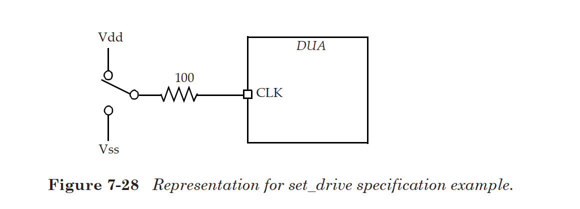
set_drive(obsolete and not recommended )
set_drive通过指定输入引脚的驱动电阻来设定drive strength。驱动电阻值越大驱动能力越弱,驱动电阻值越小驱动能力越强,缺省条件下默认驱动能力为无穷大,input pin transition time为0.
set_drive 100 UCLK
# Specifies a drive resistance of 100 on input UCLK.
# Rise drive is different from fall drive:
set_drive -rise 3 [all_inputs]
set_drive -fall 2 [all_inputs]
输入端口的驱动电阻值被用来计算第一个cell的transition time及从input port到first cell的delay time。
Delay_to_first_gate = (drive * load_on_net) + interconnect_delayset_driving_cell
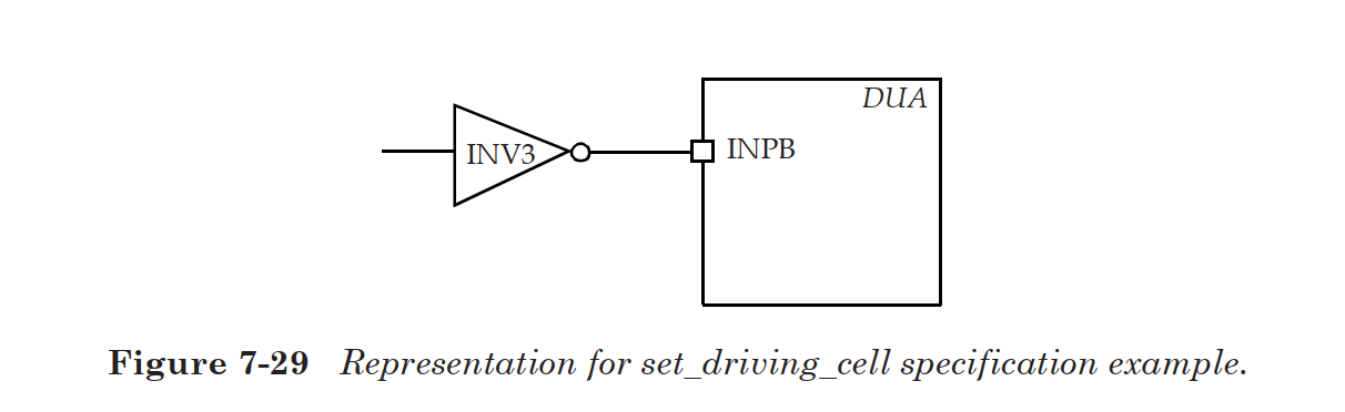
set_driving_cell可以指定输入端口的驱动单元
set_driving_cell -lib_cell INV3 -library slow [get_ports INPB]
# The input INPB is driven by an INV3 cell from library slow.

set_driving_cell -lib_cell INV2 -library tech13g [all_inputs]
# Specifies that the cell INV2 from a library tech13g is the driving cell for all inputs.

set_driving_cell -lib_cell BUFFD4 -library tech90gwc [get_ports {testmode[3]}]
# The input testmode[3] is driven by a BUFFD4 cell from library tech90gwc.
set_input_transition
set_load