在eetop上有好多好东西啊:
Silvaco_TCAD_中文教程1
不过这个教程里是Linux系统的,而且工艺仿真占了比较大的篇幅。
defect region=1 nta=5e17 wta=0.172 nga=5e15 wga=2 ntd=0.0 wtd=0 ngd=0 wgd=0

interface QF=-2e10 S.I
model fermi

solve init
solve vdrain=10
log outf=tft.log
solve vgate=-20 vstep=-0.5 vfinal=20 name=gate outfile=oxideTFT.str

tonyplot -overlay oxideTFT.str tft.log
因为之前出现了内存不足的问题,于是精简了defect的定义,步长改成了0.5,但是这样的话求解不收敛,如下。

步长改为0.1还是不收敛;
翻了下书,改了计算方法
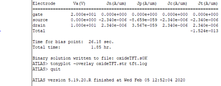
method gummel newton
可能是因为步长比较小的原因,算了好久。
输出的转移曲线如下:

emmmmmm
没想明白关态电流为啥这么高。
接下来,要手调参数拟合。
材料定义:
material material=igzo eg300=3.5 nc300=8.5e21 nv300=8.5e21 taun0=1e-9 taup0=1e-9 affinity=4.35 mup=1 mun=35
eg300:禁带宽度
nc300/nv300:effective density of states for electrons and holes
taun0/taup0:electron and hole lifetimes(载流子寿命)
affinity:电子亲和势
mup/mun:electron and hole mobilities(两种载流子的迁移率)
缺陷定义:
defect region=1 nta=5e17 wta=0.172 nga=5e15 wga=2 ntd=0.0 wtd=0 ngd=0 wgd=0
Atlas User's Manual V1 Density Of States Model
NTA/NTD:Conduction and valence band edge intercept densities
WTA/WTD:Characteristic decay energy of NTA
NGA/NGD:Total density of states
WGA/WGD:Characteristic decay energy of NGA
EGA/EGD:Peak energy/peak distribution
界面电荷定义:
interface QF=-2e10 S.I
The INTERFACE statement is used to define the interface charge density and surface recombination velocity at interfaces between semiconductors and insulators .
该语句用于定义半导体和绝缘层之间的界面电荷密度和表面复合速度。
其他的明天再说...