In this blog, I want take a different approach and describe the technical challenge encountered while bench characterizing the OPA857, a dedicatedtransimpedance amplifier (TIA) with two internal gain settings operating on a +3.3 V supply supporting a minimum of 100MHz bandwidth.
Besides the combination of both high-gain (5kΩ and 20kΩ) and high-bandwidth (>100MHz over temperature and process variation), the most challenging characteristic of the OPA857 is the need for low input capacitance requirement. This requirement, including the board parasitic, is to have the total input capacitance less than 1.5pF. Just as a clarification, the 1.5pF of total input capacitance does not include the package or the transistors parasitic. This value was selected because the OPA857 is driven by a photodiode whose biasing voltage is high enough to have the photodiode capacitance contribution between 0.5pF and 0.7pF, leaving between 0.8pF to 1pF for external parasitic.
OPA857 introduction
The OPA857 is a dedicated TIA with pseudo-differential output. The block diagram is provided in figure 1 below.
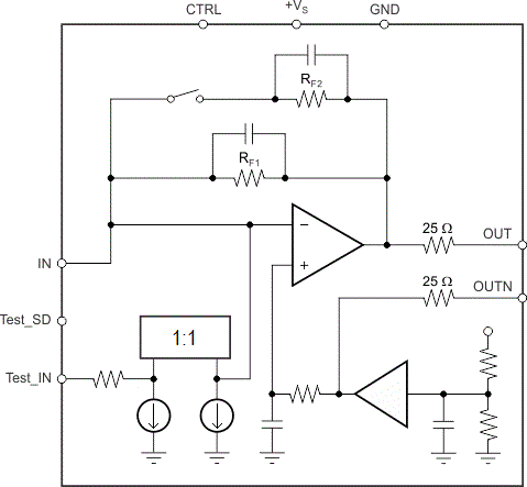
Figure 1: OPA857 block diagram
There are three distinct blocks in this diagram:
- Transimpedance block
- Reference voltage block
- Current mirror block (test block)
The transimpedance block has two selectable gain configurations: 4.5kΩ and 18.2kΩ when taking into consideration the attenuation due to a 500Ω load. Since there is only one switch, the parallel combination of the RF2 with RF1 is 4.5kΩ. The schematic is simplified to ensure that the resulting value is represented clearly.
The transimpedance block was designed to provide excellent bandwidth (>100MHz) in both gain configurations with the lowest possible RMS noise over its entire bandwidth.
The reference voltage block has several purposes:
- Provide the adequate DC-reference voltage to the input.
- Provide a DC-reference at the output allowing the DC-coupled solution to fully differential signal chain, which in turn provides CMRR as well as converting PSRR issue into CMRR.
The third block available on the pinout is intended to simplify the characterization and the evaluation of the OPA857. Before going further in this device feature and how to characterize it, let’s have a look at the expected measured performance. One of the requirements is to measure as directly as possible in the intended application circuit.
- Frequency response
- Pulse response
- Harmonic Distortion
Reference block
The reference block is set to be 5/9th of the power supply. So for 3.3 V, the reference voltage is 1.8 V. The high bandwidth allows low output impedance to high frequencies. The reference voltage is then fed to two paths. One path leading to the output OUTN has a 25Ω series resistor. The other path has a series RC going to the non-inverting input of the TIA. The RC filter is used to minimize the high frequency noise coming from the reference voltage at the buffer input.
TIA block
The amplifier of the TIA block has a class-A output stage, limiting its swing down from the common-mode voltage of 1.83 V almost all the way to the rail. Due to the internal protection, added for both protection and the improved overdrive recovery, it is not possible to swing closer to the rail than 0.6V. This still leave 1.2 V swing on the output for the dynamic range, corresponding to a maximum input current of 60uA in the 20kΩ gain and 240uA in the 5kΩ gain.
A 25Ω series resistance is also found on each output, limiting the loading the amplifier experiences, but also reduces the gain. With a 500Ω differential load, the attenuation due to the load is 0.83dB, which impacts the overall transimpedance gain. Due to the load attenuation, the 20kΩ transimpedance gain is reduced to an effective 18.2kΩ while the 5kΩ is reduced to an effective 4.5kΩ.
Bandwidth consideration
Due to its fixed transimpedance configuration and associated internal compensation, the source input capacitance must stay low as stated earlier. The nominal design target is 1.5pF including board parasitic. It is not recommended to have an input capacitance in excess of 5pF for maximum flatness in the 5kΩ gain. At 5pF input capacitance, the OPA857 in the 20kΩ gain will peak 1.5dB. See figure 2a) and 2b) below:
Figure 2: a) 20kΩ gain, b) 5kΩ gain
Note also that the bandwidth will vary with the load: the heavier the load, the lower the bandwidth. See figure 3 below.
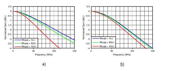
Figure 3: OPA857 bandwidth variation with load, a) 20kΩ, b) 5kΩ
Now that we have reviewed the expected performance of the amplifier, in my next post we can look into actually implementing the measurements.