流水线利用非阻塞赋值赋予的是上一时钟周期寄存器的值,来实现对寄存器的依次更新值。如:
always @ ( posedge CLK )
begin
//A[m]表示,一维数组A 中第m 个元素。
//A[m][n]表示,一维数组A 中第m 个元素,第n 位。
A[0] <= A_input; // 从外部读取新的A 值
A[1] <= A[0] | 4'b0001; // 读取A[0]值,并且设置第0 位,然后赋予A[1]
A[2] <= A[1] | 4'b0010; // 读取A[1]值,并且设置第1 位,然后赋予A[2]
A[3] <= A[2] | 4'b0100; // 读取A[2]值,并且设置第2 位,然后赋予A[3]
A[4] <= A[3] | 4'b1000; // 读取A[3]值,并且设置第3 位,然后赋予A[4]
end
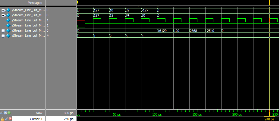
虽然在一个时钟周期内,但完成A[4]的赋值仍需要5个时钟周期,这正是非阻塞赋值的特性,每次只能更新一次上一个时钟沿寄存器的值。虽然第一次需要5个时钟周期完成,但下一个数据的处理按照时钟的概念,依次进入某一拍子中进行处理,以后的数据处理将不需再等待所谓数据的“潜伏期”。如下图所示:当经过4个潜伏期之后,便会连续的输出结果。
顶层.v文件,例化方式采用位置例化方法,注意端口次序的先后对应:


  1 module Stream_Line_Lut_Multiplier
  2 (
  3     input CLK,
  4      input RSTn,
  5
  6      input [7:0]A,
  7      input [7:0]B,
  8
  9      output [15:0]Product
 10
 11 );
 12
 13     /********************/
 14
 15      wire [8:0]U1_I1_Out;
 16      wire [8:0]U1_I2_Out;
 17
 18      task1_module U1( CLK, RSTn, A, B, U1_I1_Out, U1_I2_Out );
 19
 20      wire [7:0]U2_I1_Out;
 21      wire [7:0]U2_I2_Out;
 22
 23      task2_module U2( CLK, RSTn, U1_I1_Out, U1_I2_Out, U2_I1_Out, U2_I2_Out );
 24
 25      wire [15:0]Q1_Sig;
 26      wire [15:0]Q2_Sig;
 27
 28      lut_module U3a( CLK, U2_I1_Out, Q1_Sig );
 29      lut_module U3b( CLK, U2_I2_Out, Q2_Sig );
 30
 31      /*************************/
 32
 33      assign Product = Q1_Sig + ( ~Q2_Sig + 1'b1 );
 34
 35      /*************************/
 36
 37 endmodule
 38
 39 module task1_module
 40 (
 41
 42      input CLK,
 43      input RSTn,
 44
 45      input [7:0]A,
 46      input [7:0]B,
 47
 48      output [8:0]I1_Out,
 49      output [8:0]I2_Out
 50
 51 );
 52
 53      /***************************/
 54
 55      reg [8:0]I1;
 56       reg [8:0]I2;
 57
 58       always @ ( posedge CLK or negedge RSTn )
 59           if( !RSTn )
 60                 begin
 61
 62                       I1 <= 9'd0;
 63                         I2 <= 9'd0;
 64
 65                  end
 66            else
 67                 begin
 68
 69                      I1 <= { A[7], A } + { B[7], B };
 70                       I2 <= { A[7], A } + { ~B[7], ( ~B + 1'b1 ) };
 71
 72                  end
 73
 74     /***************************/
 75
 76      assign I1_Out = I1;
 77      assign I2_Out = I2;
 78
 79      /***************************/
 80
 81 endmodule
 82
 83
 84
 85 module task2_module
 86 (
 87     input CLK,
 88      input RSTn,
 89
 90      input [8:0]I1_In,
 91      input [8:0]I2_In,
 92
 93     output [7:0]I1_Out,
 94      output [7:0]I2_Out
 95 );
 96
 97     /************************/
 98
 99      reg [8:0]I1;
100      reg [8:0]I2;
101
102      always @ ( posedge CLK or negedge RSTn )
103          if( !RSTn )
104               begin
105
106                     I1 <= 9'd0;
107                      I2 <= 9'd0;
108
109                 end
110           else
111               begin
112
113                     I1 <= I1_In[8] ? ( ~I1_In + 1'b1 ) : I1_In;
114                      I2 <= I2_In[8] ? ( ~I2_In + 1'b1 ) : I2_In;
115
116                 end
117
118     /************************/
119
120      assign I1_Out = I1[7:0];
121      assign I2_Out = I2[7:0];
122
123      /************************/
124
125 endmodule
LUT_Rom存放的数据:
 1 0    0    1      2     4        6    9    12
 2 16    20    25    30    36    42    49    56
 3 64    72    81    90    100    110    121    132
 4 144    156    169    182    196    210    225    240
 5 256    272    289    306    324    342    361    380
 6 400    420    441    462    484    506    529    552
 7 576    600    625    650    676    702    729    756
 8 784    812    841    870    900    930    961    992
 9 1024    1056    1089    1122    1156    1190    1225    1260    1296    1332    1369    1406    1444    1482    1521    1560    1600    1640    1681    1722    1764    1806    1849    1892    1936    1980    2025    2070    2116    2162    2209    2256    2304    2352    2401    2450    2500    2550    2601    2652    2704    2756    2809    2862    2916    2970    3025    3080    3136    3192    3249    3306    3364    3422    3481    3540    3600    3660    3721    3782    3844    3906    3969    4032    4096    4160    4225    4290    4356    4422    4489    4556    4624    4692    4761    4830    4900    4970    5041    5112    5184    5256    5329    5402    5476    5550    5625    5700    5776    5852    5929    6006    6084    6162    6241    6320    6400    6480    6561    6642    6724    6806    6889    6972    7056    7140    7225    7310    7396    7482    7569    7656    7744    7832    7921    8010    8100    8190    8281    8372    8464    8556    8649    8742    8836    8930    9025    9120    9216    9312    9409    9506    9604    9702    9801    9900    10000    10100    10201    10302    10404    10506    10609    10712    10816    10920    11025    11130    11236    11342    11449    11556    11664    11772    11881    11990    12100    12210    12321    12432    12544    12656    12769    12882    12996    13110    13225    13340    13456    13572    13689    13806    13924    14042    14161    14280    14400    14520    14641    14762    14884    15006    15129    15252    15376    15500    15625    15750    15876    16002    16129    16256
10
实验过程出现的问题:
1、前些天刚做过LUT乘法实验,同样查表是用ROM生成的,但这次好几次都是输出全0.
问题所在:生成ROM的过程中,器件选型要与工程所用器件一直。
2、使用quartus中TestBench的向导Processing->start->Start TestBench Template Writer时,前提要在设置中设置好仿真工具Modelsim Altera,才能进行模版的生成。
收获:模版生成貌似挺有用的说,利用模版里边的端口映射模块,可以很简单的用在模块例化的端口映射中,这在端口量很大的工程中很能提高效率。O(∩_∩)O哈哈~
3、用Modelsim仿真发现,通过调用ROM来实现查表与直接写一个.v的ROM文件相比,前者比后者多了一个潜伏期,这是为何?
问题所在:在ROM配置的第二页最上边部分,有“What ports should be registered?”选项,意为哪些端口需要被寄存器寄存一拍,输出不要选中。此时,ROM时序示例图如图所示: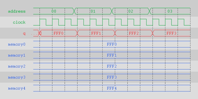
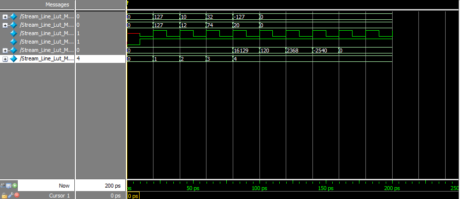
此时潜伏期变成了3个时钟周期,如下图:
4、更改ROM配置后,出现以下错误:
address :Input Warning Input port expression (1 bits) is smaller than the input port (8 bits) it drives. Extra input bit(s) "address[7..1]" will be connected to GND.
clock :Input Warning Input port expression (8 bits) is wider than the input port (1 bits) it drives. The 7 most-significant bit(s) in the expression will be dangling if they have no other fanouts.
原因:因为采用位置关联法,新配置ROM过后,需要重新调整上述ROM中和clock的顺序。
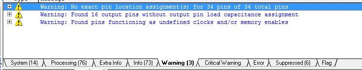
5、以下这些错误是绝对可以忽视的。
6、为什么点了时序仿真输出结果不对?(全零)
解决: