scan cell有两种不同的input:
1)data input:由电路的combinational logic驱动;
2)scan input:由另一个scan cell驱动,从而形成scan chain;
在normal/capture mode下,data input来驱动output;
在shift mode下,scan input来驱动output;
几种scan_cell:muxed-D scan,clockd-scan,level-sensitive scan design(LSSD);
muxed-D Scan cell:多指edge_triggered muxed-D scan cell,由一个D flip-flop和一个multiplexer组成,
scan enable(SE)用来选择data input和scan input的输入。

一个level-sensitive的muxed-D scan cell,由一个multiplexer,一个D Latch,一个D FF。
来用替代一个普通的latch

Clocked-scan cell:
也主要用来替代D-FF,不过是通过两个独立的clk来进行选择,
一个data clock DCK;一个shift clock SCK;
主要的优势是不会对data path的timing造成影响,但是要求多一个clock的routing。

LSSD scan cell:
主要是应用在level_sensitive,latch-based design中。
cell包含两个latch,一个master latch,一个slave latch。
其中A/B/D均为clock,D为data input,I为scan input。
优点是可以保证race-free,但是同样会增加clock的routing。

scan architecture
1)full-scan design:所有的storage element都转变为scan cell,combinational ATPG来生成test;
主要的优点是将sequential的ATPG转变为简单的combinational ATPG;
almost full-scan design:在某些critical path和insignificant path上不加入scan。
Muxed-D Full-Scan Design:
Clocked Full-Scan Design:与Muxed-D类似,只是不再使用SE,分别使用两个clock。
LSSD Full-Scan Design:两个时钟C1/C2,A/B来控制shift和capture两种mode。

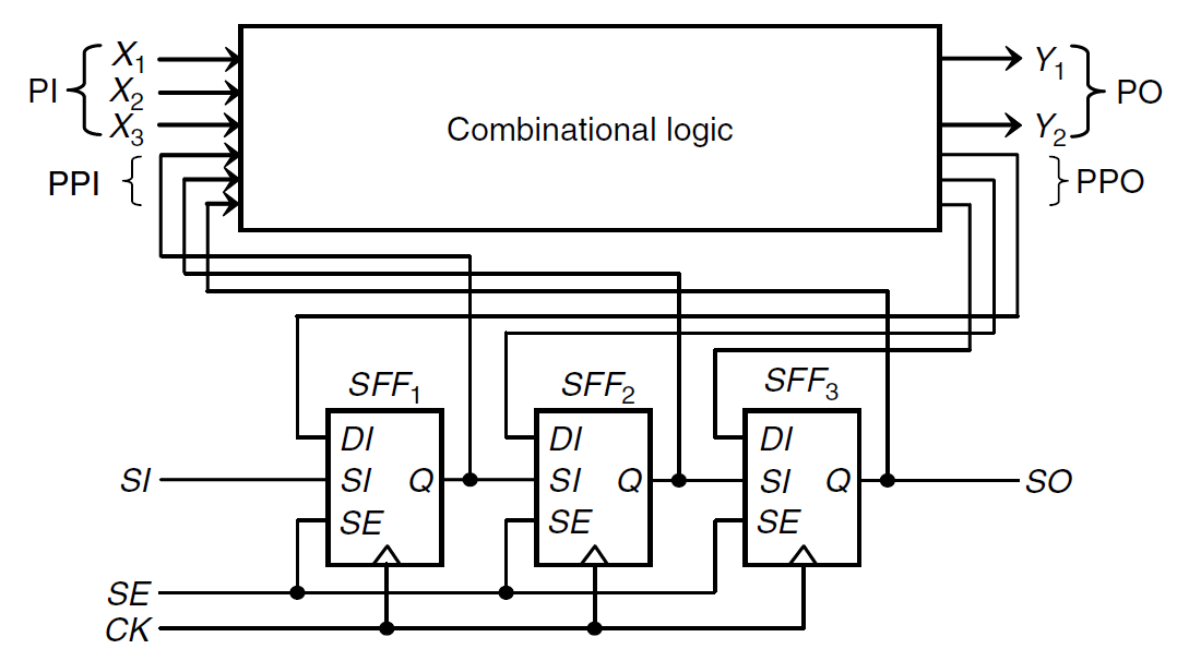
在full-scan的logic中,输入由两种:
primary input(PI),电路的external input;
pseudo primary input(PPI),scan cell的output
两种输出:
primary output(PO),电路的external output;
pseudo primary output(PPO),scan cell的input;

2)partial-scan design:部分的storage element转变为scan cell,combination和sequential ATPG来生成test;
在test的生成过程中,sequential的ATPG必须包含non-scan的FF的control和observe,这会增加test generation的
复杂性,所以一般将逻辑分开,可以根据functional partition,pipeline/feed_forward partial design.
Full-scan,partitial-scan都被定义为serial scan design,优点是routing的成本会比较低,缺点是每一个单独的scan-cell不能
在不影响本scan chain的其他cell的前提下,完成shift mode,造成high switchingde power消耗。
Random-access scan通过类似RAM似的地址寻址的方式来完成一个cell的shift mode。
3)random-access scan design:不用serial scan chain,使用random addressing的机制;
Scan cell的Q端与下一级的Scan cell的SI端直接连接起来。同时另一个load到combinational logic中。
在capture过程中,必须控制clock的个数,保证ATPG生成的reponse是正确的。
每一条scan chain中的激励和响应的reg的位置并不是对应的。根据ATPG生成的为准。