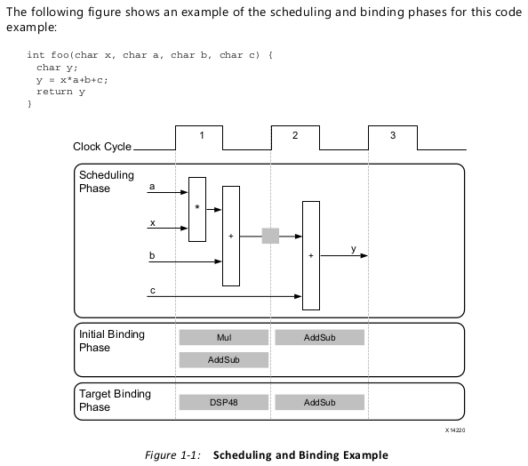
High-level synthesis includes the following phases:
•Scheduling
Determines which operations occur during each clock cycle based on:
° Length of the clock cycle or clock frequency
° Time it takes for the operation to complete, as defined by the target device
° User-specified optimization directives
If the clock period is longer or a faster FPGA is targeted, more operations are completed
within a single clock cycle, and all operations might complete in one clock cycle.
Conversely, if the clock period is shorter or a slower FPGA is targeted, high-level
synthesis automatically schedules the operations over more clock cycles, and some
operations might need to be implemented as multicycle resources.
•Binding
Determines which hardware resource implements each scheduled operation. To
implement the optimal solution, high-level synthesis uses information about the target
device.
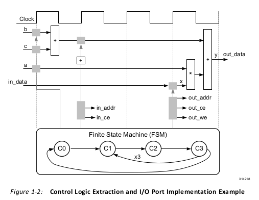
•Control logic extraction
Extracts the control logic to create a finite state machine (FSM) that sequences the
operations in the RTL design.
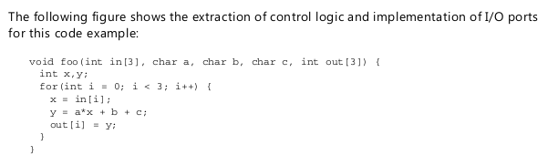
High-level synthesis synthesizes the C code as follows:
• Top-level function arguments synthesize into RTL I/O ports
• C functions synthesize into blocks in the RTL hierarchy
If the C code includes a hierarchy of sub-functions, the final RTL design includes a
hierarchy of modules or entities that have a one-to-one correspondence with the
original C function hierarchy. All instances of a function use the same RTL
implementation or block.
•Loops in the C functions are kept rolled by default
When loops are rolled, synthesis creates the logic for one iteration of the loop, and the
RTL design executes this logic for each iteration of the loop in sequence. Using
optimization directives, you can unroll loops, which allows all iterations to occur in
parallel.
•Arrays in the C code synthesize into block RAM or UltraRAM in the final FPGA design
If the array is on the top-level function interface, high-level synthesis implements the
array as ports to access a block RAM outside the design.
High-level synthesis creates the optimal implementation based on default behavior,
constraints, and any optimization directives you specify. You can use optimization directives
to modify and control the default behavior of the internal logic and I/O ports. This allows
you to generate variations of the hardware implementation from the same C code.
To determine if the design meets your requirements, you can review the performance
metrics in the synthesis report generated by high-level synthesis. After analyzing the
report, you can use optimization directives to refine the implementation. The synthesis
report contains information on the following performance metrics:
• Area: Amount of hardware resources required to implement the design based on the
resources available in the FPGA, including look-up tables (LUT), registers, block RAMs,
and DSP48s.
• Latency: Number of clock cycles required for the function to compute all output values.
• Initiation interval (II): Number of clock cycles before the function can accept new input
data.
• Loop iteration latency: Number of clock cycles it takes to complete one iteration of the
loop.
• Loop initiation interval: Number of clock cycle before the next iteration of the loop
starts to process data.
• Loop latency: Number of cycles to execute all iterations of the loop.
Reference:
1.Xilinx UG902