使用Block Memory进行PS和PL的数据交互或者数据共享,通过zynq PS端的Master GP0端口向BRAM写数据,然后再通过PS端的Mater GP1把数据读出来,将结果打印输出到串口终端显示。
涉及到AXI BRAM Controller 和 Block Memery Generator等IP的使用。
本文所使用的开发板是zedboard
PC 开发环境版本:Vivado 2016.2 Xilinx SDK 2016.2
---------------------
作者:wangdaling
来源:CSDN
原文:https://blog.csdn.net/rzjmpb/article/details/50365915 https://blog.csdn.net/rzjmpb/article/details/50365915
一、实现的结构原理图

1、PL端硬件架构搭建
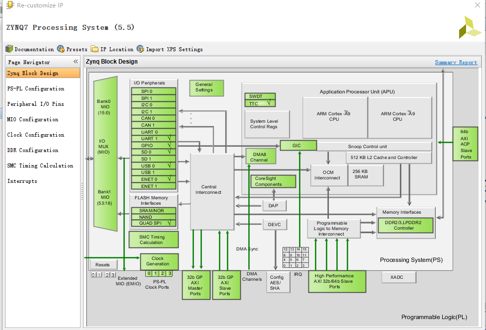
新建工程后在Create Block Design中添加IP,点击添加IP的按钮后在弹出的搜索框中搜索ZYNQ时添加PS,搜索BRAM时添加AXI BRAM Controller 和Block Memory Generator,然后对PS中的相应接口做参数设置
2、软件SDK中的代码如下:
#include <stdio.h>
#include "platform.h"
#include "xparameters.h"
#include"xparameters_ps.h"
#include"xil_printf.h"
#include"xil_io.h"
//#define DDR_BASEARDDR XPAR_DDR_MEM_BASEADDR+0x10000000
int main()
{
init_platform();
int i;
int rev;
xil_printf("-----The test is start...
");
for(i=0;i<15;i++)
{
Xil_Out32(XPAR_BRAM_0_BASEADDR+i*4,0x10000000+i);
}
for(i=0;i<15;i++)
{
rev=Xil_In32(XPAR_BRAM_0_BASEADDR+i*4);
xil_printf("the address at %x data is: %x
",XPAR_BRAM_0_BASEADDR+i*4,rev);
}
xil_printf("-----The test is end!-------
");
cleanup_platform();
return 0;
}
3、编译软件部分的代码,
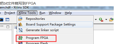
4、将zedboard 板子的JTAG和PROG的端口与PC电脑端相连
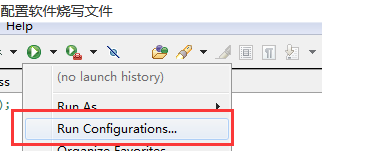
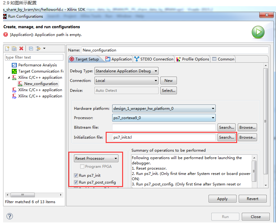
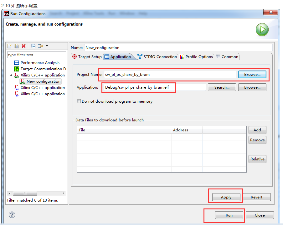
5、然后program FPGA(从硬件部分生成的bitstream),run configuration,run