板子使用的是黑金的是xilinx spartan—6开发板,首先准备一份24LC04B芯片资料,读懂资料后列出关键参数。
如下:
1、空闲状态为SDA和SCL都为高电平
2、开始状态为:保持SCL,SDA高电平不变,SDA 保持最少4us,之后SDA为低,保持最少4us
3、结束状态为:保持SCL为高、SDA为低电平不变,保持最少4us,SDA为高保持最少4us
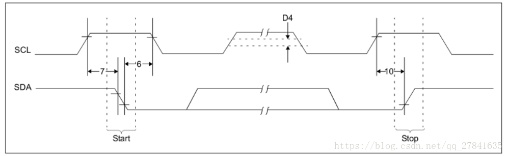
4、时间间隔4us要求来源(上面数据为24LC04,下面数据为24LC04B)
初步估算了一下时钟要求,100k(10us)符合要求,由于start有效位是在SCL高电平中间,所以SCL的上升沿和下降沿之间可以假设2个时钟周期,由上升沿触发,之后可以开始写程序了。
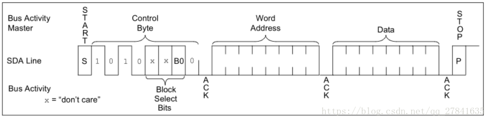
一、写流程
写寄存器的标准流程为:
1. Master发起START
2. Master发送I2C addr(7bit)和w操作0(1bit),等待ACK
3. Slave发送ACK
4. Master发送reg addr(8bit),等待ACK
5. Slave发送ACK
6. Master发送data(8bit),即要写入寄存器中的数据,等待ACK
7. Slave发送ACK
8. 第6步和第7步可以重复多次,即顺序写多个寄存器
9. Master发起STOP
二、数据写入芯片时间
由芯片资料得到3ms,为了方便程序中设置为4ms,其中为了方便调试,放入了很多测试点以及led灯显示。
三、读流程
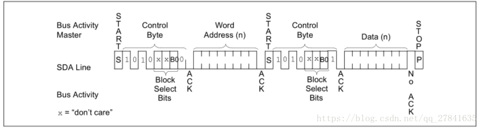
1. Master发送I2Caddr(7bit)和 w操作0(1bit),等待ACK
2. Slave发送ACK
3. Master发送reg addr(8bit),等待ACK
4. Slave发送ACK
5. Master发起START
6. Master发送I2C addr(7bit)和R读1位,等待ACK
7. Slave发送ACK
8. Slave发送data(8bit),即寄存器里的值
9. Master发送ACK
10. 第8步和第9步可以重复多次,即顺序读多个寄存器
四、程序
top和iic文件,时钟文件自己写吧,采用10us为周期的时钟。
top文件
`timescale 1ns / 1ps
module model(
CLK_50M,
reset,
led,
SDA,SCL,
clk_1s,
clk_100ms,
clk_10ms,
clk_1ms,
clk_10us,
bit_state,
write_down,read_down,
test0,test1,test2,test3,test4,test5,test6,test7,test8,test9,
read_data
);
input CLK_50M,reset;
output SCL,write_down,read_down,test0,test1,test2,test3,test4,test5,test6,test7,test8,test9;
output [3:0]led;
output [7:0]bit_state;
output [7:0]read_data;
inout SDA;
output clk_1s,clk_100ms,clk_10ms,clk_1ms,clk_10us;
//output [3:0] led;
//output [5:0] sel;
//output [7:0] LED;
wire clk_1s,clk_100ms,clk_10ms,clk_1ms,clk_10us;
//分析仪采样频率
clkdiv u0(.reset (reset),
.CLK_50M (CLK_50M),
.clkout (clk_1s),
.clkout1 (clk_100ms),
.clkout2 (clk_10ms),
.clkout3 (clk_1ms),
.clkout4 (clk_10us)
);
wirte_iic u1(
.clk_10us (clk_10us),
.reset (reset),
.led (led),
.SDA (SDA),
.SCL (SCL),
.bit_state (bit_state),
.write_down (write_down),
.read_down (read_down),
.test0 (test0),
.test1 (test1),
.test2 (test2),
.test3 (test3),
.test4 (test4),
.test5 (test5),
.test6 (test6),
.test7 (test7),
.test8 (test8),
.test9 (test9),
.read_data (read_data)
);
/***************************/
//chipscope icon和ila, 用于观察信号//
/***************************/
wire [35:0] CONTROL0;
wire [255:0] TRIG0;
chipscope_icon icon_debug (
.CONTROL0(CONTROL0) // INOUT BUS [35:0]
);
chipscope_ila ila_filter_debug (
.CONTROL(CONTROL0), // INOUT BUS [35:0]
// .CLK(dma_clk), // IN
.CLK(clk_10us), // IN, chipscope的采样时钟
.TRIG0(TRIG0) // IN BUS [255:0], 采样的信号
//.TRIG_OUT(TRIG_OUT0)
);
assign TRIG0[0] = test0; //采样
assign TRIG0[1] = test1; //采样
assign TRIG0[2] = test2; //采样
assign TRIG0[3] = test3; //采样
assign TRIG0[4] = test4; //采样
assign TRIG0[5] = test5; //采样
assign TRIG0[6] = test6; //采样
assign TRIG0[7] = test7; //采样
assign TRIG0[8] = test8; //采样
assign TRIG0[9] = test9; //采样
assign TRIG0[10] = read_down; //采样
assign TRIG0[11] = write_down; //采样
assign TRIG0[12] = SDA; //采样
assign TRIG0[13] = clk_1ms; //采样
assign TRIG0[21:14] = bit_state;
assign TRIG0[29:22] = read_data; //采样
//采样
endmodule
iic文件
`timescale 1ns / 1ps
module wirte_iic( clk_10us,
reset,
led,
SDA,
SCL,
bit_state,
write_down,
test0,test1,test2,test3,test4,,test5,test6,test7,test8,test9,
read_data,
read_down
);
input clk_10us,reset;
inout SDA;
output SCL;
output reg [3:0]led;
output reg [7:0]bit_state;//bit_state为第几个信号 ,byte_state
output reg write_down,read_down,test0,test1,test2,test3,test4,test5,test6,test7,test8,test9;
output reg [7:0]read_data;
reg SCL;
reg isOut,tx_SDA;
reg [1:0]cnt;
reg [4:0]byte_state;
reg [7:0]write_data;
reg [16:0] buf_time;//stop后,需要至少3ms写入页
parameter write_address =8'b1010_0000,
write_chipaddress =8'b0000_0000,
write_bit =8'b0001_1000;
assign SDA = isOut ? tx_SDA : 1'bz;
always @(posedge clk_10us or negedge reset)
begin
if(!reset)
cnt <=0;
else begin
if(cnt ==3)
cnt <=0;
else
cnt <= cnt +1'b1;
end
end
always @(posedge clk_10us or negedge reset)
begin
if(!reset)begin
tx_SDA <=0;
SCL <=0;
isOut <=0;
led<=4'b0000;
bit_state <=0;
byte_state <=0; //第几个8位包
write_data <=0;
write_down <=0;
read_down <=0;
read_data <=0;
test0<=0;test1<=0;test2<=0;test3<=0;test4<=0;
test5<=0;test6<=0;test7<=0;test8<=0;test9<=0;
buf_time<=0;
end
else if(write_down==0&&read_down==0) begin
case (bit_state)
0:begin//起始位
if(cnt==0)begin tx_SDA<=1;SCL<=1;isOut <=1;end
if(cnt==1)begin tx_SDA<=1;SCL<=1;end
if(cnt==2)begin tx_SDA<=0;SCL<=1;end
if(cnt==3)begin tx_SDA<=0;SCL<=0;bit_state<=bit_state +1;write_data<=write_address; end
end
1,2,3,4,5,6,7,8:begin//数据写入
if(cnt==0)begin SCL<=0; tx_SDA <= write_data[8-bit_state];isOut <=1;end //高位先发送
if(cnt==1)begin SCL<=1;end
if(cnt==2)begin SCL<=1;end
if(cnt==3)begin SCL<=0;bit_state <= bit_state +1;end
end
9:begin//判断ACK
if(cnt==0)begin isOut<=0; end //释放SDA
if(cnt==1)begin SCL<=1;end
if(cnt==2)begin
if(SDA==0&&byte_state==0)begin
byte_state <=1;write_data<=write_chipaddress;end
else if(SDA==0&&byte_state==1)begin
byte_state <=2;write_data<=write_bit;end
else if(SDA==0&&byte_state==2)begin
byte_state <=3;write_data<=write_address; end
else begin SCL<=1;end
end
if(cnt==3)begin
if(byte_state==1)begin
SCL<=0;bit_state<=1;end
else if(byte_state==2)begin
SCL<=0;bit_state<=1; end
else if(byte_state==3)begin
SCL<=0;bit_state<=10;end
else begin SCL<=0; end
end
end
10:begin//停止位
if(cnt==0)begin tx_SDA<=0;SCL<=0;isOut<=1;end
if(cnt==1)begin tx_SDA<=0;SCL<=1;end
if(cnt==2)begin tx_SDA<=1;SCL<=1;end
if(cnt==3)begin tx_SDA<=1;SCL<=0;bit_state<=11; end
end
11:begin//缓存3ms写入数据
if(cnt==0)begin tx_SDA<=1'bz;SCL<=1'bz;isOut<=0;end
if(cnt==1)begin tx_SDA<=1'bz;SCL<=1'bz;end
if(cnt==2)begin tx_SDA<=1'bz;SCL<=1'bz;end
if(cnt==3)begin
if(buf_time==100)begin
write_down <=1;
bit_state<=0; end
else begin
bit_state<=11;
buf_time<=buf_time+1;end
end
end
default:begin isOut <=0;led<=4'b1111; end
endcase
end
else if(write_down==1&&read_down==0)begin//读取数据
case(bit_state)
0:begin//起始位
if(cnt==0)begin tx_SDA<=1;SCL<=1;isOut <=1;end
if(cnt==1)begin tx_SDA<=1;SCL<=1;end
if(cnt==2)begin tx_SDA<=0;SCL<=1;end
if(cnt==3)begin tx_SDA<=0;SCL<=0;bit_state<=bit_state +1;
if(byte_state==5)write_data<=8'b10100001;else write_data<=write_address;end
end
1,2,3,4,5,6,7,8:begin//数据写入
if(cnt==0)begin SCL<=0; tx_SDA <= write_data[8-bit_state];isOut <=1;end//高位先发送
if(cnt==1)begin SCL<=1;end
if(cnt==2)begin SCL<=1;end
if(cnt==3)begin SCL<=0;bit_state <= bit_state +1;end
end
9:begin//判断ACK
if(cnt==0)begin isOut<=0;end //释放SDA
if(cnt==1)begin SCL<=1; end
if(cnt==2)begin
if(SDA==0&&byte_state==3)begin
byte_state <=4;write_data<=write_chipaddress;end
else if(SDA==0&&byte_state==4)begin
byte_state <=5; end
else if(SDA==0&&byte_state==5)begin
byte_state <=6; end
else begin SCL<=1;end
end
if(cnt==3)begin
if(byte_state==4)begin
SCL<=0;bit_state<=1;end
else if(byte_state==5)begin
SCL<=0;bit_state<=0; end
else if(byte_state==6)begin
SCL<=0;bit_state<=10;end
else begin SCL<=0; end
end
end
10,11,12,13,14,15,16,17:begin//数据读
if(cnt==0)begin SCL<=0; isOut<=0; end
if(cnt==1)begin SCL<=1;end
if(cnt==2)begin
if(byte_state==6)begin
SCL<=1;
read_data[17-bit_state] <= SDA;end
end
if(cnt==3)begin SCL<=0;bit_state <= bit_state +1;end
end
18:begin//NACK to 1
if(cnt==0)begin SCL<=0;isOut<=0; end
if(cnt==1)begin SCL<=1;end
if(cnt==2)begin
if(SDA==1)begin
SCL<=1;end
else begin SCL<=1;bit_state<=0;end
end
if(cnt==3)begin SCL<=0; bit_state <= bit_state +1; end
end
19:begin//stop
if(cnt==0)begin tx_SDA<=0;SCL<=0;isOut<=1;end
if(cnt==1)begin tx_SDA<=0;SCL<=1;end
if(cnt==2)begin tx_SDA<=1;SCL<=1;end
if(cnt==3)begin tx_SDA<=1;SCL<=0;bit_state <= bit_state +1; end
end
20:begin//空闲信号只能在边沿变化,同步非常重要
if(cnt==0)begin tx_SDA<=1;SCL<=1;isOut<=1;end
if(cnt==1)begin tx_SDA<=1;SCL<=1; end
if(cnt==2)begin tx_SDA<=1;SCL<=1; end
if(cnt==3)begin read_down<=1;bit_state<=0; led<=4'b0001;end
end
default:begin isOut <=0;end
endcase
end
else if(write_down==1&&read_down==1)begin
if(cnt==0)begin tx_SDA<=1;SCL<=1;isOut<=0;end
if(cnt==1)begin tx_SDA<=1;SCL<=1; end
if(cnt==2)begin tx_SDA<=1;SCL<=1; end
if(cnt==3)begin tx_SDA<=1;SCL<=1; end
end
else begin led<=4'b1111;end
end
endmodule