参考:
ug906 Vivado Design Suite User Guide Design Analysis and Closure Techniques
--------------
CLKC #1 Advisory The MMCME3 cell sgmii_top_sync_ins2/pcs_instance_1/inst/core_clocking_i/mmcme3_adv_inst has COMPENSATION value BUF_IN, but CLKOUT0 output drives sequential cells directly connected to ports. In order to achieve insertion delay and phase-alignment for the sequential cells directly connected to ports, a COMPENSATION of ZHOLD must be used. (The problem cell is rst_n_IBUF_inst/IBUFCTRL_INST (in rst_n_IBUF_inst macro).)
CLKC #3 Advisory The MMCME3_ADV cell sgmii_top_sync_ins6/pcs_instance_1/inst/core_clocking_i/mmcme3_adv_inst CLKIN1 or CLKIN2 pin is driven by global Clock buffer(s) sgmii_top_sync_ins6/bufg_ins_e_clk125 and does not have a LOC constraint. It is recommended to LOC the MMCM and use the CLOCK_DEDICATED_ROUTE constraint on the net(s) driven by the global Clock buffer(s).

CLKC #1 The MMCME3 cell refclk/inst/mmcme3_adv_inst has COMPENSATION value ZHOLD, but CLKOUT1 output drives sequential IO cells. In order to achieve insertion delay and phase-alignment for the IO sequential cells, CLKOUT0 must be used.

[DRC PDRC-153] Gated clock check: Net sgmii_top_sync_ins1/u1/smi_config_inst/smi_inst/mdio_en__0 is a gated clock net sourced by a combinational pin sgmii_top_sync_ins1/u1/smi_config_inst/smi_inst/mdio_en_reg_i_2/O, cell sgmii_top_sync_ins1/u1/smi_config_inst/smi_inst/mdio_en_reg_i_2. This is not good design practice and will likely impact performance. For SLICE registers, for example, use the CE pin to control the loading of data.

-------------------------------------------------------------------------------------------------
#set_property CLOCK_DELAY_GROUP cdg0 [get_nets -of [get_pins -hier -filter {name =~  *core_clocking_i/clk312_buf/O}]]
set_property CLOCK_DELAY_GROUP cdg0 [get_nets -of [get_pins -of [get_cells -hierarchical -filter {NAME =~ *core_clocking_i/clk312_buf}] -filter {REF_PIN_NAME =~ O}]]
#set_property CLOCK_DELAY_GROUP cdg0 [get_nets -of [get_pins -hier -filter {name =~  *core_clocking_i/clk625_buf/O}]]
set_property CLOCK_DELAY_GROUP cdg0 [get_nets -of [get_pins -of [get_cells -hierarchical -filter {NAME =~ *core_clocking_i/clk625_buf}] -filter {REF_PIN_NAME =~ O}]]

设计中保留了未使用的寄存器:

-------------------------------------------------------------------------
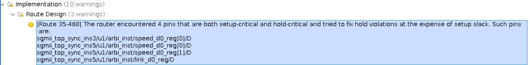
插入跨时钟域xpm消除时序违例及警告:


------------------------------------------------------------------------------------------------
--------------------------------------------------------------------------------------------------


-----------------------------------------------------------

MIG接口必需要求在同一个SLR上:

解决办法: