1、在手册 中 找到 SPI 相关 文档
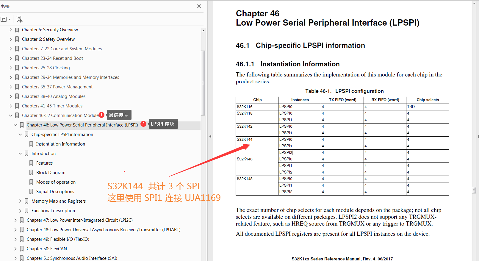
2、SPI 相关 说明
46.4.1.1 Functional clock
The LPSPI functional clock is asynchronous to the bus clock and if it remains enabled in
low power modes then LPSPI can perform SPI bus transfers and low power wakeups in
both master and slave modes. The LPSPI divides the functional clock by a prescaler and
the resulting frequency must be at least two times faster than the SPI external clock
(LPSPI_SCK) frequency.
功能时钟
LPSPI功能时钟与总线时钟异步,如果保持启用状态,
在低功耗模式下,LPSPI可以在以下情况下执行SPI总线传输和低功耗唤醒:
主模式和从模式。 LPSPI将功能时钟除以预分频器,然后
产生的频率必须至少比SPI外部时钟快两倍
(LPSPI_SCK)频率。
46.4.1.2 External clock
The LPSPI shift register is clocked directly by the LPSPI_SCK clock that is either
generated internally in master mode or supplied externally in slave mode.
LPSPI移位寄存器由LPSPI_SCK时钟直接计时,该时钟为
在主机模式下内部产生或在从机模式下外部提供。
46.4.1.3 Bus clock
The bus clock is only used for bus accesses to the control and configuration registers. The
bus clock frequency must be sufficient to support the data bandwidth requirements of the
LPSPI registers, including FIFOs.
46.4.1.3总线时钟
总线时钟仅用于总线访问控制和配置寄存器。 的
总线时钟频率必须足以支持数据总线的数据带宽要求
LPSPI寄存器,包括FIFO。
46.4.1.4 Chip reset
The logic and registers for the LPSPI are reset to their default state on a chip reset.
46.4.1.4芯片复位
LPSPI的逻辑和寄存器在芯片复位时复位为默认状态。
46.4.1.5 Software reset
The LPSPI implements a software reset bit in the Control Register. The CR[RST] will
reset all logic and registers to their default state, except for the CR itself.
46.4.1.5软件重置
LPSPI在控制寄存器中实现软件复位位。 CR [RST]将
将所有逻辑和寄存器重置为默认状态,CR本身除外。
46.4.1.6 FIFO reset
The LPSPI implements write-only control bits that resets the transmit/command FIFO
(CR[RTF] and receive FIFO (CR[RRF]). A FIFO is empty after being reset.
46.4.1.6 FIFO复位
LPSPI实现只写控制位,该位复位发送/命令FIFO
(CR [RTF]和接收FIFO(CR [RRF])。FIFO复位后为空。
三:主机模式 功能讲解
46.4.2.1 Transmit and Command FIFO
The transmit and command FIFO is a combined FIFO that includes both transmit data
and command words. Command words are stored to the transmit/command FIFO by
writing the transmit command register. Transmit data words are stored to the transmit/
command FIFO by writing the transmit data register.
发送和命令FIFO是组合的FIFO,其中包括发送数据
和命令字。 命令字通过以下方式存储到发送/命令FIFO中
写入发送命令寄存器。 发送数据字被存储到发送/
通过写入发送数据寄存器来命令FIFO。
When a command word is at the top of the transmit/command FIFO, the following
actions can occur:
• If the LPSPI is between frames, the command word is pulled from the FIFO and
controls all subsequent transfers.
当命令字位于发送/命令FIFO的顶部时,以下内容
可能发生的动作:
• If the LPSPI is busy and either the existing CONT bit is clear or the new CONTC
value is clear, the SPI frame will complete at the end of the existing word, ignoring
the FRAMESZ configuration. The command word is then pulled from the FIFO and
controls all subsequent transfers (or until the next update to the command word).
•如果LPSPI忙,并且现有的CONT位清零或新的CONTC
值清除后,SPI帧将在现有字的末尾完成,而忽略
FRAMESZ配置。 然后将命令字从FIFO中拉出并
控制所有后续传输(或直到下一次更新命令字)。
• If the LPSPI is busy and the existing CONT bit is set and the new CONTC value is
set, the command word is pulled from the FIFO during the last LPSPI_SCK pulse of
the existing frame (based on FRAMESZ configuration) and the frame continues
using the new command value for the rest of the frame (or until the next update to the
command word). When CONTC is set, only the lower 24-bits of the command word
are updated.
置位时,在最后一个LPSPI_SCK脉冲期间,命令字从FIFO中拉出。
现有框架(基于FRAMESZ配置),并且框架继续
在其余帧中使用新的命令值(或直到下一次更新
命令字)。 设置CONTC时,仅命令字的低24位
已更新。
The current state of the existing command word can be read by reading the transmit
command register. It requires at least three LPSPI functional clock cycles for the transmit
command register to update after it is written (assuming an empty FIFO) and the LPSPI
must be enabled (CR[MEN] is set).
可以通过读取发送来读取现有命令字的当前状态
命令寄存器。 发送至少需要三个LPSPI功能时钟周期
命令寄存器在写入后(假定为空FIFO)和LPSPI进行更新
必须启用(设置CR [MEN])。
Writing the transmit command register does not initiate a SPI bus transfer, unless the
TXMSK bit is set. When TXMSK is set, a new command word will not be loaded until
the end of the existing frame (based on FRAMESZ configuration) and the TXMSK bit
will be cleared at the end of the transfer.
写入发送命令寄存器不会启动SPI总线传输,除非
TXMSK位置1。 设置TXMSK时,直到加载新命令字
现有帧的末尾(基于FRAMESZ配置)和TXMSK位
将在转帐结束时清除。
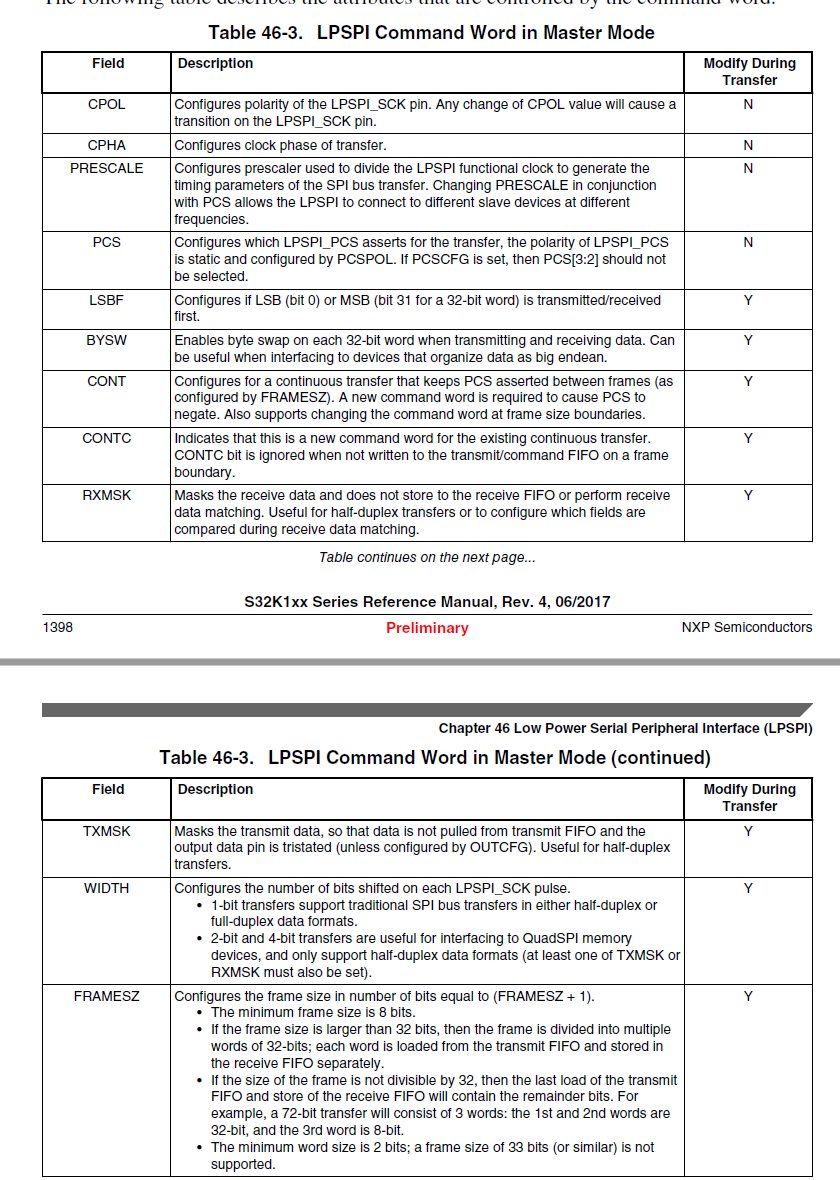
The following table describes the attributes that are controlled by the command word.
下表描述了由命令字控制的属性。
The LPSPI initiates a SPI bus transfer when data is written to the transmit FIFO, the
HREQ pin is asserted (or disabled) and the LPSPI is enabled. The SPI bus transfer uses
the attributes configured in the transmit command register and timing parameters from
the clock configuration register to perform the transfer. The SPI bus transfer ends once
the FRAMESZ configuration is reached, or at the end of a word when a new transmit
command word is at the top of the transmit/command FIFO. The HREQ input is only
checked the next time the LPSPI goes idle (completes the current transfer and transmit/
command register is empty).
当数据写入发送FIFO时,LPSPI启动SPI总线传输。
HREQ引脚被置为有效(或禁用)并且LPSPI被使能。 SPI总线传输使用
传输命令寄存器中配置的属性和来自
时钟配置寄存器执行传输。 SPI总线传输一次结束
达到FRAMESZ配置,或在新传输时在单词末尾
命令字在发送/命令FIFO的顶部。 HREQ输入仅
下次LPSPI处于空闲状态时进行了检查(完成当前传输和发送/
命令寄存器为空)。
The transmit/command FIFO also supports a Circular FIFO feature. This allows the
LPSPI master to (periodically) repeat a short data transfer that can fit within the transmit/
command FIFO, without requiring additional FIFO accesses. When the circular FIFO is
enabled, the current state of the FIFO read pointer is saved and the status flags do not
update. Once the transmit/command FIFO is considered empty and the LPSPI is idle, the
FIFO read pointer is restored with the saved version, so the contents of the transmit/
command FIFO are not permanently pulled from the FIFO while circular FIFO mode is
enabled.
发送/命令FIFO还支持循环FIFO功能。 这允许
LPSPI主站(周期性地)重复进行一次短数据传输,使其适合发送/
命令FIFO,而无需其他FIFO访问。 当循环FIFO为
启用后,将保存FIFO读取指针的当前状态,并且不保存状态标志
更新。 一旦发送/命令FIFO被认为是空的并且LPSPI处于空闲状态,则
FIFO读取指针与保存的版本一起恢复,因此发送/接收的内容
在循环FIFO模式下,命令FIFO不会从FIFO中永久拉出
已启用。
46.4.2.2 Receive FIFO and Data Match
The receive FIFO is used to store receive data during SPI bus transfers. When RXMSK is
set, receive data is discarded instead of storing in the receive FIFO.
46.4.2.2接收FIFO和数据匹配
接收FIFO用于在SPI总线传输期间存储接收数据。 当RXMSK为
设置后,接收数据将被丢弃,而不是存储在接收FIFO中。
The receive data is written to the receive FIFO at the end of the frame. During a multiple
word or continuous transfer, the receive data is also written to the receive FIFO at the
same time as new transmit data is read from the transmit FIFO. If the transmit FIFO is
empty during a continuous transfer, the receive data is only written to the receive FIFO
after the transmit FIFO is written or the command register is written to end the frame.
Receive data supports a receive data match function that can match received data against
one of two words or against a masked data word. The data match function can also be
configured to compare only the first one or two received data words since the start of the
frame. Receive data that is already discarded due to RXMSK bit cannot cause the data
match to set and will delay the match on first received data word until after all discarded
data is received. The receiver match function can also be configured to discard all receive
data until a data match is detected, using the CFGR0[RDMO] control bit. When clearing
the CFGR0[RDMO] control bit following a data match, clear CFGR0[RDMO] before
clearing SR[DMF] to allow all subsequent data to be received.
接收数据在帧的末尾写入接收FIFO。在多次
字或连续传输时,接收数据也将在以下位置写入接收FIFO:
与从发送FIFO中读取新的发送数据的时间相同。如果发送FIFO为
在连续传输期间为空,接收数据仅写入接收FIFO
在写入发送FIFO或写入命令寄存器以结束帧之后。
接收数据支持接收数据匹配功能,可以将接收到的数据与
两个字之一或针对屏蔽数据字。数据匹配功能也可以是
配置为仅比较自开始以来的第一个或两个接收到的数据字
帧。接收由于RXMSK位已被丢弃的数据不会导致数据
设置匹配项,将延迟对第一个接收到的数据字的匹配,直到全部丢弃
数据已接收。接收器匹配功能也可以配置为丢弃所有接收
使用CFGR0 [RDMO]控制位,直到检测到数据匹配为止。清理时
数据匹配之后的CFGR0 [RDMO]控制位,在清除CFGR0 [RDMO]之前
清除SR [DMF]以允许接收所有后续数据。
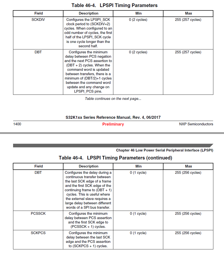
46.4.2.3 Timing Parameters
The following table lists the timing parameters that are used for all SPI bus transfers,
these timing parameters are relative to the LPSPI functional clock divided by the
PRESCALE configuration. Although the Clock Configuration Register cannot be
changed when the LPSPI is busy, the PRESCALE configuration can be altered between
transfers using the command register, to support interfacing to different slave devices at
different frequencies.
46.4.2.3时序参数
下表列出了用于所有SPI总线传输的时序参数,
这些时序参数相对于LPSPI功能时钟除以
PRESCALE配置。 虽然时钟配置寄存器不能
如果在LPSPI繁忙时更改了PRESCALE配置,则可以在
使用命令寄存器进行传输,以支持与不同从设备的接口
不同的频率。
46.4.2.4 Pin Configuration
The LPSPI_SIN and LPSPI_SOUT pins can be configured via the PINCFG configuration
to swap directions or even support half-duplex transfers on the same pin.
The OUTCFG configuration can be used to determine if output data pin (eg:
LPSPI_SOUT) will tristate when the LPSPI_PCS is negated, or if it will simply retain the
last value. When configuring for half-duplex transfers using the same data pin in single
bit transfer mode, or any transfer in 2-bit and 4-bit transfer modes, then the output data
pins must be configured to tristate when LPSPI_PCS is negated.
The PCSCFG configuration is used to disable LPSPI_PCS[3:2] functions and to use them
for quad-data transfers. This option must be enabled when performing quad-data
transfers.
可以通过PINCFG配置来配置LPSPI_SIN和LPSPI_SOUT引脚
交换方向,甚至在同一引脚上支持半双工传输。
OUTCFG配置可用于确定输出数据引脚(例如:
当LPSPI_PCS取反时,或者如果仅保留LPSPI_PCS,LPSPI_SOUT)将进入三态。
最后的值。 在单个配置中使用相同的数据引脚配置半双工传输时
位传输模式,或2位和4位传输模式下的任何传输,然后输出数据
LPSPI_PCS取反时,必须将引脚配置为三态。
PCSCFG配置用于禁用LPSPI_PCS [3:2]功能并使用它们
用于四元数据传输。 执行四元数据时必须启用此选项
转移。
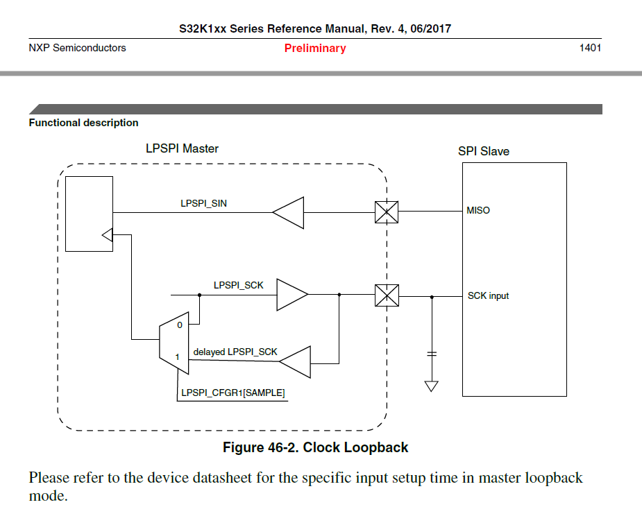
46.4.2.5 Clock Loopback
The LPSPI master can be configured to use one of two clocks to sample the input data
(eg: LPSPI_SIN), either the LPSPI_SCK output clock directly or a delayed version of
this clock. The delayed version of the LPSPI_SCK is delayed by the LPSPI_SCK pin
output delay, plus the LPSPI_SCK pin input delay, and is configured by setting
CFGR1[SAMPLE]. Enabling the loopback version of the LPSPI_SCK can improve the
setup time of the input data from the slave.
46.4.2.5时钟环回
可以将LPSPI主器件配置为使用两个时钟之一来采样输入数据
(例如:LPSPI_SIN),可以直接使用LPSPI_SCK输出时钟,也可以使用延迟版本
这个时钟。 LPSPI_SCK的延迟版本由LPSPI_SCK引脚延迟
输出延迟加上LPSPI_SCK引脚输入延迟,通过设置
CFGR1 [SAMPLE]。 启用LPSPI_SCK的环回版本可以改善
从站输入数据的建立时间。
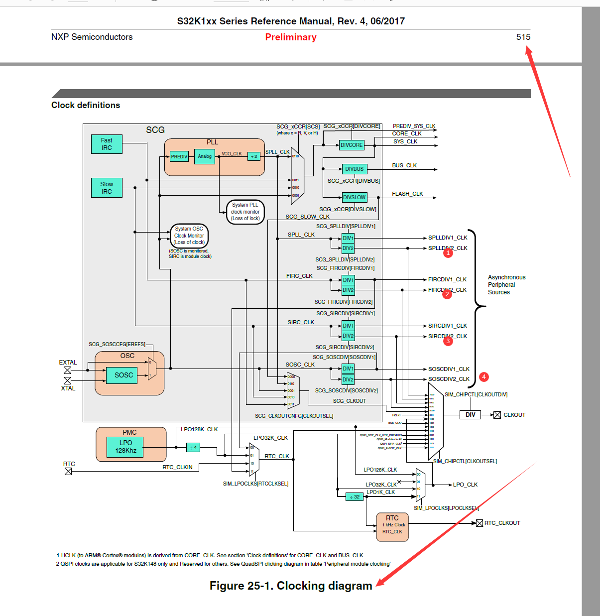
四:SPI 时钟源 选择
四种 时钟源 来源