Must tri-state outputs and use an external resistor to pull up to 5V
To drive 5V CMOS-level inputs, a pull-up resistor must be applied to the 5V Virtex output. Prior
to driving a logic 1 data signal, the Virtex output must be tri-stated. This ensures no overlap or
crowbar current in the input buffers of the 5V-receiving device.
The required Virtex output pin configuration is commonly called “open collector”, or more
correctly, “open drain”. This function is easily generated inside the chip by driving the data
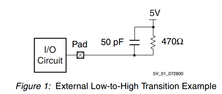
together with the active low Output Enable signal of the output block. The external low-to-high
transition is then driven only by the pull-up resistor. For example, applying a 470-ohm pull-up
resistor to 5V and a 50-pF load capacitance (as shown in Figure 1) creates a 0.4V to 4.5V rise
time of about 40 ns.
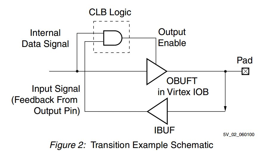
For a faster rise time, the internal active low Output Enable signal is not driven directly from the
internal data signal. Instead, it is driven from a two-input AND gate that is driven by both the
internal data signal and the input signal returned from the same device’s output pin. On the
rising edge, this assures that the output pull-up transistor is active for most of the rise time,
resulting in a shorter output delay. The important part of the rise time from 0.4V to 3.0V is
reduced dramatically, from 20 ns to 3 ns (see Figure 2).
Ringing can be avoided by following proper board design practices. In most cases, the fast
active edge enables the CMOS threshold to be passed with a propagation delay of less than 3
ns. At worst, an additional pullup from the resistor is still needed to reach the threshold voltage
reliably, but this enables at least 15 ns to be saved.