http://electronicdesign.com/power/simple-addition-permits-voltage-control-dc-dc-converters-output
In a standard dc-dc converter, a resistor divider typically defines a fixed output voltage. However, applications like programmable output voltage power supplies and motor control circuits require dynamic control of the dc-dc converter’s output voltage. The circuit described here allows control of the converter’s output voltage, VOut, with a control voltage, VC.
In a conventional dc-dc buck converter, VOut is:

so VOut is fixed by the values of R1 and R2 (Fig. 1).
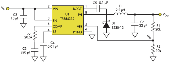
1. The output voltage in a conventional dc-dc buck converter is fixed and depends on the resistor divider, R1/R2.
The added circuitry in Figure 2 enables users to control the same dc-dc converter’s output voltage using VC.
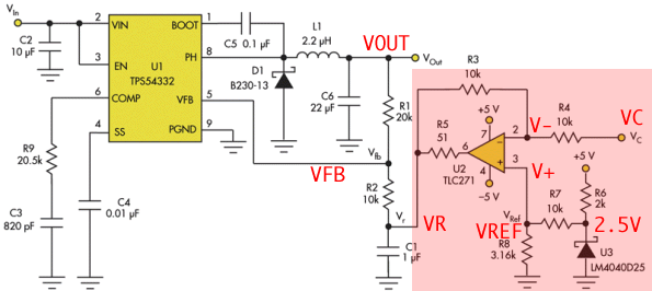
In this case, R2 is not connected to the ground but, rather, to Vr. Equation 1 then becomes:
VOUT = VFB + ( ( VFB - VR ) / R2 ) * R1
VOUT - VR = VFB - VR + ( ( VFB - VR ) / R2 ) * R1
VOUT - VR = ( VFB - VR ) * R2 / R2 + ( VFB - VR ) * R1 / R2
VOUT - VR = ( VFB - VR ) * ( R2 + R1 ) / R2

Since R1 = 20 kΩ and R2 = 10 kΩ, Equation 2 can be simplified to:
VOut – Vr = 3(Vfb – Vr)(3)
or:
VOut = 3 Vfb – 2 Vr(4)
( VC - V- ) / R4 = ( V- - VR ) / R3 ( I4 = I3 )
VC / R4 - V- / R4 = V- / R3 - VR / R3
V- / R4 + V- / R3 = VC / R4 + VR / R3
V- * ( R3 + R4 ) / ( R3 * R4 ) = ( VC * R3 + VR * R4 )/ ( R3 * R4 )
V- * ( R3 + R4 ) = ( VC * R3 + VR * R4 )
VR * R4 = V- * ( R3 + R4 ) - VC * R3
V- = V+ = VREF : VR * R4 = VREF * ( R3 + R4 ) - VC * R3
R3 = R4 : VR * R3 = VREF * ( R3 + R3 ) - VC * R3
VR = VREF * 2 - VC
R3 and R4 have the same value, 10 kΩ, so amplifier U2’s output voltage is:
Vr = 2 VRef – VC(5)
where VRef is the reference voltage generated by U3 after resistor divider R7/R8.
VOut = 3 Vfb – 2 Vr(4)
Combining Equation 4 and Equation 5:
VOut = 3 Vfb – 4 VRef + 2 VC (6)
To simplify Equation 6, choose components that make:
3 Vfb = 4 VRef(7)
Then Equation 6 becomes:
VOut = 2 VC (8)
The internal voltage reference of U1 is 0.8 V. ( TPS54332 )
VREF = 3VFB / 4 = 3 *0.8 / 4 = 0.6V
LM4040D25 : 2.5V : By choosing R7 = 10 kΩ and R8 = 3.16 kΩ, VRef = 0.6 V, satisfying Equation 7.
Finally, C1 lowers U2’s output impedance at high frequencies,
maintaining the stability of U1’s feedback loop.
The added circuitry allows users to control the buck converter’s output voltage,
VOut, in the range of 0 to 5 V with a control voltage, VC, in the range of 0 to 2.5 V.
Similar circuitry can be designed for use with a boost converter,
or any other dc-dc converter, as long as its feedback voltage pin is accessible.
Using an operational amplifier in the feedback path
A very flexible way of influencing the feedback pin while not being so restricted
in terms of the control signal is to use an operational amplifier.
It can be used to inject some current into the feedback divider which then
forces the control loop of the power supply to change the output voltage.
This way the output voltage can be varied continuously as a function
of the current injected into the feedback node.
Often, the information controlling the output voltage change on a power supply in sensor applications
as well as motor drive applications is an analog signal.
Depending on the nature of this control signal, the circuit around the operational amplifier
can be defined to set the lowest voltage output independent of what the control signal range is.
Also there is great flexibility in the ratio of control signal change to change in the output voltage.
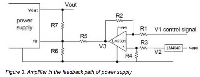
Figure 3 shows an amplifier circuit in the feedback path of a switching power supply.
The difference amplifier uses an operational amplifier and four additional resistors R1 through R4.
The output of the operational amplifier acts like a voltage source.
In order to inject a current into the feedback node this voltage is converted into a current by resistor R5.
It equals the internal impedance of the current source which the operational amplifier and R5 constitute.
Together with the feedback resistors R6 and R7 any output voltage changes
can be set based on almost any given control signal.
The signal voltage V1 is the control signal.
The voltage V2 is a reference voltage for the operational amplifier.
It should be a fairly constant voltage since variations on it will
change the output voltage of the power supply as well.
If a fairly precise rail in the system is available it can generally be used.
A good solution is a low voltage reference IC such as National Semiconductors LM4040.