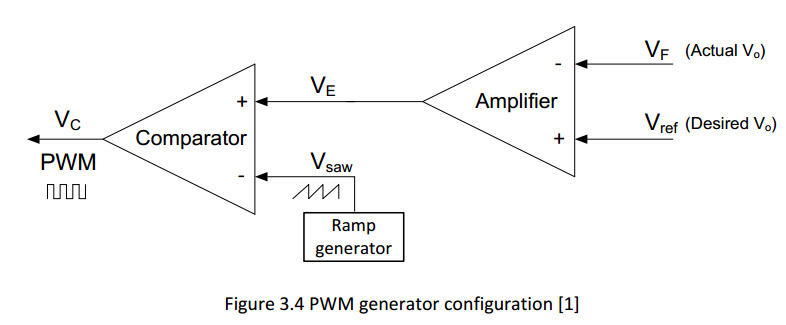
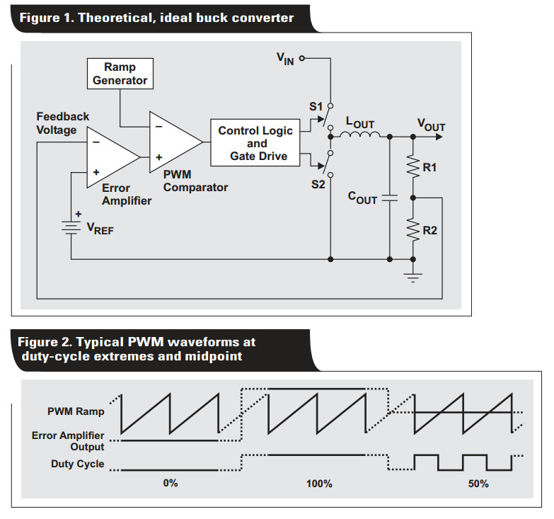
As shown in figure 3.4, PWM controller contains two main parts;
voltage error-amplifier and voltage comparator.
The error-amplifier compares the feedback voltage VF (applied to inverting input)
to reference voltage VREF (applied to non-inverting input)
then their difference which is called voltage error signal VE
after amplification is applied to noninverting input of voltage comparator.
Comparator compares this error voltage to sawtooth ramp VSAM that is generated by ramp generator,
if voltage VE is higher than VSAW output voltage of comparator goes high but
when VE is lower than VSAW the output of comparator goes low
to adjust the switching duty cycle.
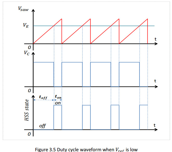
error voltage VE is inversely proportional to voltage reference VREF,
for example when VREF is low, error voltage VE is increased by error amplifier to adjust the switching duty cycle.
As can be seen in figure 3.5 when the error voltage is high the pulse width of PWM wave
at the output of voltage comparator (VC ) is increased to keep off High side switch (PMOS) for
the most time of the each cycle in order to reduce duty cycle to regulate output voltage.
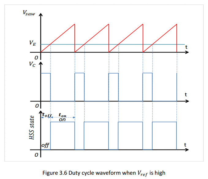
Vice versa as shown in figure 3.6 when VREF is high error amplifier reduces VE to keep on
the HSS for a most time of each period in order to adjust output voltage [14].
http://www.chinabaike.com/2011/0120/201049.html

From the derivations for the boost, buck, and inverter (flyback), it can be seen that changing the duty cycle controls the steady-state output with respect to the input voltage. This is a key concept governing all inductor-based switching circuits.
The most common control method, shown in Figure 7, is pulse-width modulation (PWM). This method takes a sample of the output voltage and subtracts this from a reference voltage to establish a small error signal (VERROR). This error signal is compared to an oscillator ramp signal. The comparator outputs a digital output (PWM) that operates the power switch. When the circuit output voltage changes, VERROR also changes and thus causes the comparator threshold to change. Consequently, the output pulse width (PWM) also changes. This duty cycle change then moves the output voltage to reduce to error signal to zero, thus completing the control loop.
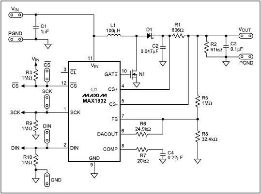
Figure 8 shows a practical circuit using the boost topology formed with the MAX1932.
This IC is an integrated controller with an onboard programmable digital-to-analog converter (DAC).
The DAC sets the output voltage digitally through a serial link.
R5 and R8 form a divider that meters the output voltage.
R6 is effectively out of circuit when the DAC voltage is the same as the reference voltage (1.25V).
This is because there is zero volts across R6 and so zero current.
When the DAC output is zero (ground), R6 is effectively in parallel with R8.
These two conditions correspond to the minimum and maximum output adjustment range of 40V and 90V, respectively.

Next, the divider signal is subtracted from the internal 1.25V reference and then amplified.
This error signal is then output on pin 8 as a current source.
This, in conjunction with the differential input pair, forms a transconductance amplifier.
This arrangement is used because the output at the error amp is high impedance (current source),
allowing the circuit's gain to be adjusted by changing R7 and C4.
This arrangement also provides the ability to trim the loop gain for acceptable stability margins.
The error signal on pin 8 is then forwarded to the comparator and output to drive the power switch.
R1 is a current-sense resistor that meters the output current.
When the current is unacceptably high, the PWM circuit shuts down, thereby protecting the circuit.
The type of switching (topology) in Figures 7 and 8 is classified as a voltage-mode controller (VMC)
because the feedback regulates the output voltage.
For analysis we can assume that if the loop gain is infinite, the output impedance for an ideal voltage source is zero.
Another commonly used type of control is current-mode control (CMC).
This method regulates the output current and, with infinite loop gain, the output is a high-impedance source.
In CMC, the current loop is nested with a slower voltage loop, as shown in Figure 9;
a ramp is generated by the slope of the inductor current and compared with the error signal.
So, when the output voltage sags, the CMC supplies more current to the load.
The advantage of CMC is its ability to manage the inductor current.
In VMC the inductor current is not metered. This becomes a problem because the inductor,
in conjunction with the output filter capacitor, forms a resonant tank that can ring and even cause oscillations.
Current mode control senses the inductor current to correct for inconsistencies.
Although difficult to accomplish, carefully selected compensation components can effectively cancel out this resonance in VCM.

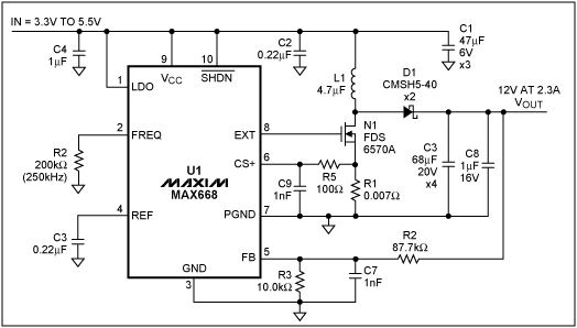
The circuit in Figure 10 uses CMC with the MAX668 controller.
This boost circuit is similar to Figures 7 and 8 except that R1 senses the inductor current for CMC.
R1 and some internal comparators provide a current limit.
R5 in conjunction with C9 filters the switching noise on the sense resistor to prevent false triggering of the current limit.
The MAX668's internal current-limit threshold is fixed; changing the resistor, R1, adjusts the current-limit setting.
The resistor, R2, sets the operating frequency.
The MAX668 is a versatile integrated circuit that can provide a wide range of DC-DC conversions.
The external components of the MAX668 can have high-voltage ratings that provide greater flexibility for high-power applications.
For portable applications that require less power, the MAX1760 and MAX8627 are recommended.
These latter devices use internal FETs, and sense the current by using the FETs' resistance to measure inductor current (no sense resistor required).