http://www.f4grx.net/projet-module-nfc/
The NFC is a contactless communication technology, which is used for transport cards and other contactless cards CB. The signal is modulated at a frequency of 13.56 MHz, which is a "ISM" band as the 2.4 GHz or 433.92 MHz. Outside the NFC, this band is used for plasma machines in physics, semiconductors, etc..
I noticed that there were few affordable hackables NFC readers.
The only one I know is OpenPCD based on a chip from NXP NFC reader. This project implements a contactless card reader whose firmware is to experiment.
I recently came across the circuit Texas Instruments TRF7970A that not only is able to function as the circuit NXP (card reader, or "initiator" in NFC language), but also in "peer to peer" mode and "target" (card emulation). This is a ridiculously small component (QFN) but easily available. Despite its small size hard soldering, it deserves interest. An evaluation kit is available from TI, but 1) I do not like the evaluation kits and 2) it is expensive (49 or 99 dollars). So I'll make my own map.
Following all the docs reference provided by TI, I was able to develop my own evaluation board, the size of 5 × 5 cm.
The first card is a suitable antenna with its matching circuit impedance: Component values are calculated according to formulas (magic for beginners) having characterized the inductance of the antenna. I will return to these calculations later.
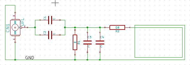
he antenna design is based on a design NXP several towers that allows for both son of antenna output on the same side.

The second card is the "drive" itself, which has a different circuit impedance, the TRF circuit and a connection to a microcontroller SPI Tiva C, the successor to the Stellaris found on the Stellaris Launchpad card.
Here are some specifications:
- Front-end NFC Texas Instruments TRF7970A
- Coaxial connector for antenna UFL
- ARM Cortex M4 microcontroller Tiva C Series TM4F123
- 256k flash
- 32k of RAM
- USB (OTG unwired, so only device)
- I2C Port
- UART
- Port JTAG header on 10 points (standard pinout ARM)
- 20 GPIO available on header 2.54mm
- 5V, USB or external

And the circuit:
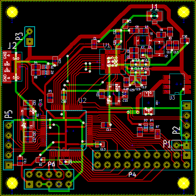
I managed to get by for very little copper tracks side, suddenly the plan covers the entire underside of the circuit. The majority of green trails you see connect all ground points to make sure I do not forget any. In reality, all these tracks are embedded in the ground plane. I use this technique to make sure my ground plane is in one piece.
