http://www.altera.com/literature/hb/max2/max2_mii51009.pdf
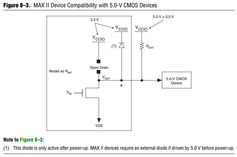
The open-drain pin never drives high, only low or tri-state. When the open-drain pin is active, it drives low.
When the open-drain pin is inactive, the pin is tri-stated and the trace pulls up to 5.0 V by the external resistor.
The purpose of enabling the I/O clamp diode is to protect the MAX II device’s I/O pins.
The 3.3-V VCCIO supplied to the I/O clamp diodes causes the voltage at point A to clamp at 4.0 V,
which meets the MAX II device’s reliability limits when the trace voltage exceeds 4.0 V.
The device operates successfully because a 5.0-V input is within its input specification.
The I/O clamp diode is only supported in the EPM1270 and EPM2210 devices’ I/O Bank 3.
An external protection diode is needed for other I/O banks in EPM1270 and EPM2210 devices
and all I/O pins in EPM240 and EPM570 devices.
The pull-up resistor value should be small enough for sufficient signal rise time,
but large enough so that it does not violate the IOL (output low) specification of MAX II devices.
The maximum MAX II device IOL depends on the programmable drive strength of the I/O output.
Table 8–1 shows the programmable drive strength settings
that are available for the 3.3-V LVTTL/LVCMOS I/O standard for MAX II devices.
The Quartus II software uses the maximum current strength as the default setting.
The PCI I/O standard is always set at 20 mA with no alternate setting.

To compute the required value of REXT, first calculate the model of the open-drain
transistors on the MAX II device. This output resistor (REXT) can be modeled by
dividing VOL by IOL (REXT = VOL/IOL). Table 8–2 shows the maximum VOL for the 3.3-V
LVTTL/LVCMOS I/O standard for MAX II devices.
f For more information about I/O standard specifications, refer to the DC and Switching
Characteristics chapter in the MAX II Device Handbook.

Select REXT so that the MAX II device’s IOL specification is not violated. You can
compute the required pull-up resistor value of REXT by using the equation: REXT =
(VCC/IOL) – RINT. For example, if an I/O pin is configured as a 3.3-V LVTTL with a 16
mA drive strength, given that the maximum power supply (VCC) is 5.5 V, the value of
REXT can be calculated as follows:

This resistor value computation assumes worst-case conditions. You can adjust the
REXT value according to the device configuration drive strength. Additionally, if your
system does not see a wide variation in voltage-supply levels, you can adjust these
calculations accordingly.
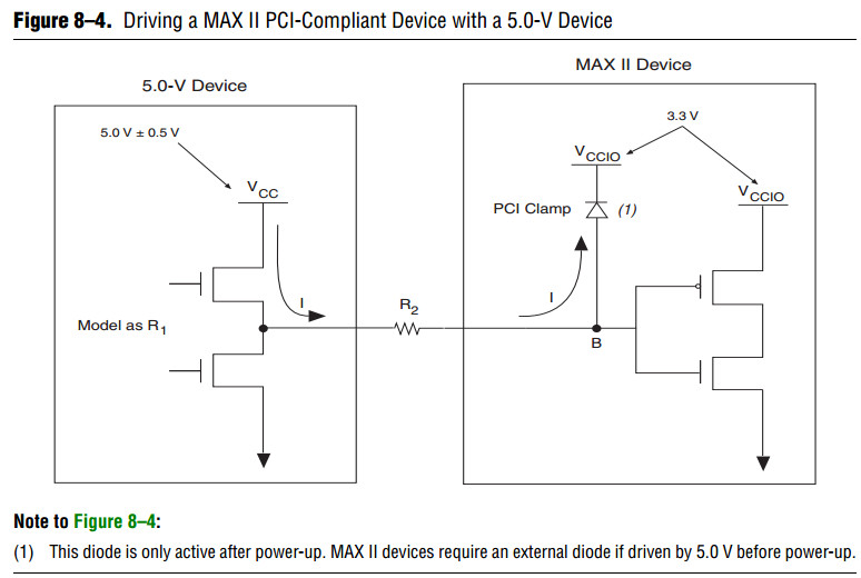
Because MAX II devices are 3.3-V, 32-bit, 66-MHz PCI compliant, the input circuitry
accepts a maximum high-level input voltage (VIH) of 4.0 V.
To drive a MAX II device with a 5.0-V device, you must connect a resistor (R2)
between the MAX II device and the 5.0-V device. See Figure 8–4.
If VCCIO for MAX II devices is 3.3 V and the I/O clamp diode is enabled, the voltage at point B in Figure 8–4 is 4.0 V,
which meets the MAX II devices reliability limits when the trace voltage exceeds 4.0 V.
To limit large current draw from the 5.0-V device, R2 should be small enough for a fast signal rise time
and large enough so that it does not violate the high-level output current (IOH) specifications of the devices driving the trace.
To compute the required value of R2, first calculate the model of the pull-up transistors on the 5.0-V device.
This output resistor (R1) can be modeled by dividing the 5.0-V device supply voltage (VCC) by the IOH: R1 = VCC/IOH
Figure 8–5 shows an example of typical output drive characteristics of a 5.0-V device.
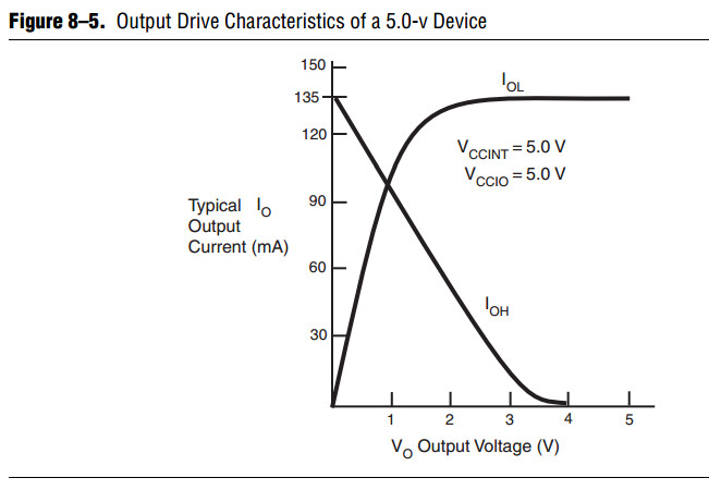
As shown above, R1 = 5.0 V/135 mA.
The values usually shown in data sheets reflect typical operating conditions.
Subtract 20% from the data sheet value for guard band.
This subtraction applied to the above example gives R1 a value of 30.
Select R2 so that the MAX II device’s IOH specification is not violated. For example,
if the above device has a maximum IOH of 8 mA, given the I/O clamp diode,
VIN = VCCIO + 0.7 V = 3.7 V.
Given that the maximum supply load of a 5.0-V device (VCC) is 5.5 V, the value of R2
can be calculated as follows:

This analysis assumes worst-case conditions. If your system does not see a wide
variation in voltage-supply levels, you can adjust these calculations accordingly.
Because 5.0-V device tolerance in MAX II devices requires use of the I/O clamp, and
this clamp is activated only after power-up, 5.0-V signals may not be driven into the
device until it is configured.
The I/O clamp diode is only supported in the EPM1270 and EPM2210 devices’ I/O Bank 3.
An external protection diode is needed for other I/O banks for EPM1270 and EPM2210 devices
and all I/O pins in EPM240 and EPM570 devices.