http://www.microchip.com/stellent/idcplg?IdcService=SS_GET_PAGE&nodeId=1824&appnote=en011794
In many applications, a DC/DC Converter is used to produce a regulated voltage or current,
derived from an unregulated power supply, or from a battery.
Examples of these applications include battery chargers, electronic air purifiers,
emergency exit signs, and distributed power systems.
In some of those applications, a dedicated Switched Mode Power Supply (SMPS) Controller IC
is used in conjunction with a microcontroller.
In other applications, however, a dedicated SMPS Controller IC may be overkill.
An alternative approach is to generate a low cost SMPS function in a smart microcontroller,
such as the PIC16C620A.
This Application Note shows a method of using the microcontroller to perform simple SMPS control functions.
Two circuits were built for evaluation.
One circuit provides a Constant Voltage output,
the other a Constant Current output
DC/DC CONVERTER

There are several popular DC/DC Converter topologies, such as the Boost and Fly-back Converter topologies.
The DC/DC Converter used in this example is a Buck (or step down) Converter, which is also a popular topology.
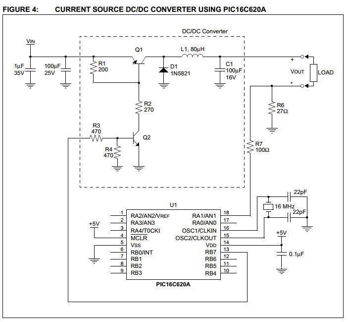
In Figure 3, the Buck Converter consists of transistor Q1, diode D1, inductor L1, and capacitor C1.
Transistor Q2 is used as a level translator for the PICmicro device PORTB output to turn Q1 on or off.
Application Note AN701 explains how a Buck Converter works. It also provides a general guideline on component selection.
In any type of DC/DC Converter circuit, the power device selections are very important.
The key parameters to look for in the transistor Q1 are the switching time and current rating.
These two parameters greatly affect the maximum switching frequency of the converter,
and also how much current the converter can be designed for.
The diode D1 should either be a Schottky, or ultra fast diode, in order to minimize switching losses in the converter.
The type of capacitor C1 is also very important to minimize the ripple on the converter output.
An electrolytic capacitor with a low ESR (Equivalent Series Resistance) is desirable for capacitor C1.
In some cases, the output ripple of the converter may still be higher than desired,
even with the proper inductor and capacitor selections.
In this case, an additional inductor and capacitor may be used as a low pass filter at the converter output.
A DC/DC Converter is normally chosen because of its high efficiency in converting the input power to output power.
Unlike a linear regulator, the efficiency measure of a DC/DC Converter generally increases as its load increases.
A properly designed DC/DC Converter can yield an efficiency measure of greater than 90% at full load.
The efficiency of a DC/DC Converter is expressed as the ratio of output power and input power.
The following equations can be used to determine efficiency

The selection of the DC/DC Converter components, in many cases, is a trade-off between cost, performance, and size.
In this Application Note, the component selections were made to simply provide a DC/DC Converter
that can be used to demonstrate the PIC16C620A capability to perform SMPS controller function.
The DC/DC Converter discussed here is not optimized for any particular parameter.
SMPS CONTROLLER FUNCTION
The DC/DC Converter circuit is merely a power processor.
It transforms the available input voltage and current into the output voltage and current,
based on the command of the SMPS controller.
The SMPS controller looks at the converter output, compares the output to a set point,
performs a control algorithm and finally, applies the algorithm output to a modulator.
The modulator output is then used to drive the DC/DC Converter.
Figure 1 shows a simplified block diagram of a complete DC/DC Converter system.
In this Application Note, the PIC16C620A is used to implement the SMPS controller function,
which includes the following functions:
set point generation,
error amplifier,
control algorithm, and
the modulator.
These functions are shown inside the dashed box in Figure 1.

MODULATOR - PULSE SKIPPING MODULATION (PSM)
One of the simplest modulation techniques used for controlling a DC/DC Converter is Pulse Skipping Modulation (PSM),
which is also known as Pulsed Frequency Modulation.
In a PSM system, the modulator generates a train of pulses to turn the converter power switch on and off.
The pulses have a fixed pulse width, as well as period.
As long as the converter output is below the desired target, the PSM pulses continue to run the converter switch.
Once the converter output reaches or exceeds the target, the next PSM pulse is skipped.
This operation will result in decreasing pulse density as the converter output reaches its target, or as the output loading decreases.
When the converter output falls below the target, or as the output loading increases, the PSM pulse density will increase.
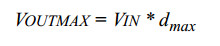
The theoretical limit of the maximum output voltage is determined by the input voltage to the DC/DC Converter
and the maximum duty cycle of the PSM signal, which is the duty cycle of the PSM signal when it is continuously running (not skipping pulses).
This relationship can be expressed as follows:
This formula does not take into account the conduction and switching losses of the converter components.
The discussion of non-ideal DC/DC Converter is beyond the scope of this Application Note.
However, many papers and text books are available on this subject.
In this application, the PIC16C620A microcontroller performs the modulator function in firmware.
This firmware modulator generates the PSM pulses on the RB7 pin (PORTB, bit 7),
to drive transistor Q2 of the DC/DC Converter.
When the DC/DC Converter output is below the desired value,
the firmware continuously sends out PSM pulses to increase the converter output.
Once the DC/DC Converter output exceeds the target, the controller will skip the PSM pulses
until the output voltage, or current, falls below the threshold and the control cycle repeats.
Timer0 of the microcontroller is used to generate a time base for the firmware modulator.
Timer0 is enabled and the TMR0 register is loaded with a reload value.
When Timer0 overflows, an interrupt occurs. In the interrupt routine, TMR0 is again loaded with the reload value.
The reload value determines the time base of the PSM signal.
In this application, the TMR0 reload value is chosen to produce a time base of 50 microseconds
when the microcontroller runs from a 16 MHz crystal. Other crystal frequencies may be used;
however, the 16 MHz was selected to give plenty of instruction cycles in between Timer0 interrupts,
for the firmware execution. When the actual application requirements are well defined,
the operating frequency can be adjusted to a lower frequency to save power
FEEDBACK CIRCUIT
For the SMPS controller to work properly, the DC/DC Converter system must include a feedback circuit.
The feedback circuit provides information to the SMPS controller of the converter output.
Feedback Circuit for Constant Voltage DC/DC Converter
The first circuit is a Constant Voltage DC/DC Converter.
The feedback requirement for a Constant Voltage control is a voltage proportional to the output voltage.
In Figure 3, this feedback circuit consists of R5 and R6.
The output of the R5-R6 divider is applied to the AN1 input pin of the C2 comparator in the PIC16C620A.
The two resistors simply scale down the output voltage to equal the reference voltage.
The formula to calculate R5 and R6 is shown below
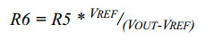
The parallel combination value of R5 and R6 should be less than 10 kΩ to minimize errors
due to input leakage current from the AN1 pin.
Some applications require that the feedback voltage can be trimmed to compensate for the VREF variations over process.
If this capability is required, then a potentiometer can be added to allow trimming.
To get the most accurate results, the adjustment of the trim potentiometer should be performed when the system is running.
Feedback Circuit for Constant Current DC/DC Converter
The second circuit is a Constant Current DC/DC Converter.
The feedback requirement for this circuit is a voltage proportional to the output current.
For the Constant Current circuit in Figure 4, the feedback consists of simply R6. The voltage on R6 is then
presented to the AN1 input pin of the C2 comparator in
the PIC16C620A. Resistor R7 is added to provide ESD
protection to the AN1 pin, since the load will be connected to R6 directly. The formula to calculate R6 is:
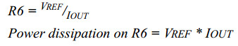
for applications where the output current is high, a very small current sense resistor, R6, is required to minimize power dissipation.
In this case, an operation amplifier may be required to amplify the small voltage on R6 to the size of VREF.
Similar to the Constant Voltage applications, depending on the need,
a trimming potentiometer may be required in the Constant Current application as well.
Since potentiometers are generally not designed to dissipate power,
it is very important to make sure that the potentiometer does not carry the load current,
for reliability and control drift minimization reasons.
Output Load Connections for the Constant Current DC/DC Converter
For the circuit shown in Figure 4, the load connections for the Constant Current circuit can not be grounded.
If the load is grounded, then the current sense resistor R6 is shorted to ground and the SMPS controller can not sense the load current.
If a grounded load is required in the system, the method for current sensing must be modified.
The following are possible solutions to allow a ground referenced load:
1. Ground the load and float the PICmicro microcontroller ground.
2. Move the current sense resistor to the output of the DC/DC Converter and use an op-amp
to level shift the voltage on R6 to a ground referred signal.
SET POINT AND VOLTAGE CONTROL ALGORITHM
The PIC16C620A has an on-board voltage reference, VREF, and two comparators, C1 and C2 (see Figure 2 for illustration).
The VREF module is used to provide a set point to the system.
If so desired, the set point voltage can be adjusted via firmware.
In this application, the VREF set point is set to VDD/2.
The comparators have several configurations, some of which allow the comparators to compare external voltage(s) to the VREF voltage.
The configuration that is used for this application example is shown in Figure 2.
To select this configuration, the comparator control register CMCON must be set to b’00000010’.
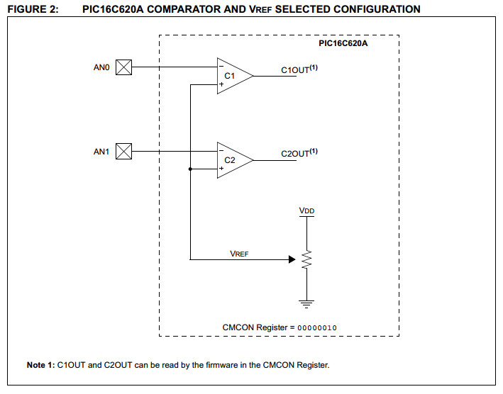
In this application, only the C2 comparator of the
PIC16C620A is used to compare the feedback voltage
on the AN1 pin to the internal voltage reference VREF.
If the DC/DC Converter output is lower than the desired
value, then the feedback voltage presented on AN1 is
lower than VREF. In this case, the comparator output,
C2OUT, is high. If the DC/DC Converter output is
higher than the desired value, then the comparator output is low. The firmware uses the comparator output
state to determine whether the DC/DC Converter output needs to be increased or not.
The Voltage Control Algorithm performed in firmware
becomes very simple:
• If the voltage on AN1 pin is lower than VREF, then
produce PSM output pulse
• Else (voltage on AN1 pin is higher than VREF),
then skip PSM output pulse
Because the PIC16C620A and the firmware monitors
and controls the voltage on the AN1 pin, regardless of
whether the voltage is derived from either the Constant
Voltage or Constant Current feedback circuit, this firmware can be used for either the Constant Voltage or
Constant Current circuit implementation without any
changes.
Integrating the Voltage Control and Modulator
The Voltage Control Algorithm is executed every time
Timer0 interrupts. After the firmware reloads TMR0, it
checks the comparator output to determine whether the
output pulse should be active or not, on the next PSM
cycle. Once this decision is made, a flag bit is set or
cleared depending on the decision, and the output
pulse is turned off. After several microseconds delay,
before leaving the interrupt routine, the output pulse is
activated again, depending on the status of the flag bit.
If the output is set, this pulse will stay active until the
next Timer0 interrupt occurs. If the output is clear, then
the PSM pulse is skipped until the next Timer0 interrupt
occurs, and the control sequence repeats. Figure 5
shows the flowchart of the Firmware SMPS Controller.


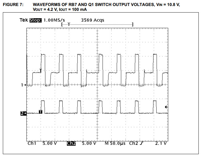
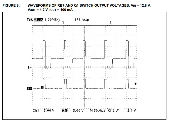
WAVEFORMS FROM THE VOLTAGE
SOURCE CIRCUIT
To see how the DC/DC Converter circuit works, voltage
waveforms of the PSM output on RB7 and the Q1
switch output are captured for 3 different input voltage
levels, while the output load is kept constant at 4.2 V,
100 mA. The RB7 PSM output voltage is shown as
Channel 1, while the Q1 switch output voltage is shown
as Channel 2. The waveforms are captured at the following input voltage levels:
1. VIN = 8.8 V. See Figure 6.
2. VIN = 10.8 V. See Figure 7.
3. VIN = 12.8 V. See Figure 8.
When the RB7 output is high, the Q1 switch turns on.
The switch output voltage immediately rises to the input
voltage, i.e., 8.8 V on Figure 6. At this time, the inductor
current increases. The inductor current is flowing to the
capacitor C1 and the DC/DC Converter load. Once the
RB7 output goes low, the Q1 switch turns off. The
inductor current, however, needs a low impedance path
to continue its flow. This causes the switch output voltage to fall until diode D1 turns on. The inductor current
now flows through the diode from the system ground.
Figure 6 shows that the voltage at the output of the
switch drops to approximately -0.7V. At this time, the
voltage across the inductor reverses its polarity, causing the inductor current to drop. When the inductor current reaches zero, diode D1 turns off, and the voltage
on the inductor collapses to zero. This can be seen by
the Q1 switch output going from -0.7V to the DC/DC
Converter output voltage.
Note that although the waveform seems repetitive, the
frequency is not constant. Once in a while, the distance
between pulses changes. This change happens when
the Voltage Control Algorithm determines that additional pulses should be skipped for that PSM cycle.
The waveforms on Figure 6, Figure 7 and Figure 8,
were taken with the same voltage and time scales. It is
obvious from looking at the three plots, as the ratio of
VIN/VOUT increases, the pulse density on the RB7 pin
decreases. At higher input voltages, each switching of
the Q1 transistor will deliver higher charge to the DC/
DC Converter output.
For a constant input voltage, the PSM pulse density on
the RB7 pin will also vary as a function on the output
load. In the Constant Voltage circuit, as the output current decreases, the PSM pulse density on the RB7 pin
also decreases.
FIGURE 6: WAVEFORMS OF RB7 AND Q1 SWITCH OUTPUT VOLTAGES, VIN = 8.8 V,
VOUT = 4.2 V, IOUT = 100 mA

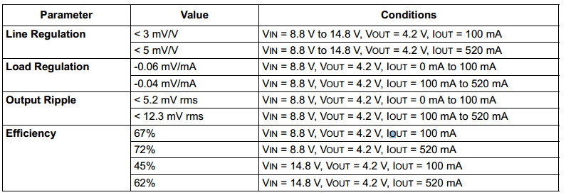
BENCH MEASUREMENTS DATA
To quantitatively evaluate performance, each circuit
was tested in the lab. Several key parameters relevant
to power supply circuits were measured. Those parameters are:
1. Line Regulation: both Constant Voltage and
Constant Current circuits.
Line regulation is the amount of change on the
output as a function of the input voltage. For the
Constant Voltage circuit, the units for line regulation are V/V, while for the Constant Current
they are A/V (or mA/V).
2. Load Regulation: both Constant Voltage and
Constant Current circuits.
Load regulation is the amount of change on the
output as a function of the load. For the Constant Voltage circuit, the units for load regulation
are V/A (or mV/mA), while for the Constant Current they are A/V (or mA/V).
3. Output Ripple Noise: Constant Voltage only.
The output ripple noise is measured in mV rms.
4. Power Conversion Efficiency: Constant
Voltage only.
The Efficiency is measured as the ratio of power
delivered to the load and power delivered to the
DC/DC Converter.
Bench Measurement Data of the Constant
Voltage DC/DC Converter
The following table is a summary of the Constant Voltage DC/DC Converter performance.
TABLE 1: CONSTANT VOLTAGE DC/DC CONVERTER PERFORMANCE
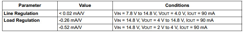
Bench Measurement Data of the Constant
Current DC/DC Converter
The following table is a summary of the Constant Current DC/DC Converter performance. The output ripple
current of this circuit was not measured. The Efficiency
parameter was also not measured. The Efficiency measure, however, should be identical to that of the Constant Voltage DC/DC Converter for a given similar input
and output condition to the circuit.
TABLE 2: CONSTANT CURRENT DC/DC CONVERTER PERFORMANCE
EXPANDING THE APPLICATION
The use of the PIC16C620A in DC/DC Converter circuits can be expanded to the following applications:
1. Constant Voltage with Current Limit DC/DC
Converters.
Since the PIC16C620A has two comparators,
one comparator can be used for the voltage
feedback, and the other for detecting current
limit.
2. Other power converter topologies.
The control methodology can be used for Boost
and Fly-back topologies, as well. The feedback
circuitry, more than likely, must be modified to
include the power switch current sensing.
3. Firmware programmable output voltage or
current.
The VREF voltage can be changed in firmware.
This capability allows user to change the output
voltage or current as needed by the application.
4. The use of other modulation techniques, i.e.,
Pulse Width Modulation (PWM).
A PWM control can be implemented, instead of
the PSM technique used in this example. In
addition to Timer0 interrupt, the comparator
interrupt is also enabled. In this case, the comparator interrupt determines when to turn off the
RB7 output pulse as soon as the control threshold is reached. In this type of PWM control, however, it is possible for the PWM signal to oscillate
when the duty cycle is greater than 50%, due to
a phenomenon called the Right Half Plane Zero.
Under this condition, a slope compensation is
required to stabilize the PWM control signal.
The detailed implementations of any of those applications are left as an exercise to the readers’ creativity.
USION
This Application Note has demonstrated that the
PIC16C620A can be used to perform simple SMPS
controller functions, such as Constant Voltage, Constant Current, or Constant Voltage with current limit.
The program example can be used with any of the
PICmicro family members, which has on-board
comparators.
REFERENCES
1. PIC16C620A Datasheet, DS30235 revision H or
newer
2. AN701: Switch Mode Battery Eliminator Based
on a PIC16C72A
  1 ;
  2 ;            Software License Agreement
  3 ;
  4 ; The software supplied herewith by Microchip Technology Incorporated
  5 ; (the 揅ompany? for its PICmicro?Microcontroller is intended and
  6 ; supplied to you, the Company抯 customer, for use solely and
  7 ; exclusively on Microchip PICmicro Microcontroller products. The
  8 ; software is owned by the Company and/or its supplier, and is
  9 ; protected under applicable copyright laws. All rights are reserved.
 10 ;  Any use in violation of the foregoing restrictions may subject the
 11 ; user to criminal sanctions under applicable laws, as well as to
 12 ; civil liability for the breach of the terms and conditions of this
 13 ; license.
 14 ;
 15 ; THIS SOFTWARE IS PROVIDED IN AN "AS IS" CONDITION. NO WARRANTIES,
 16 ; WHETHER EXPRESS, IMPLIED OR STATUTORY, INCLUDING, BUT NOT LIMITED
 17 ; TO, IMPLIED WARRANTIES OF MERCHANTABILITY AND FITNESS FOR A
 18 ; PARTICULAR PURPOSE APPLY TO THIS SOFTWARE. THE COMPANY SHALL NOT,
 19 ; IN ANY CIRCUMSTANCES, BE LIABLE FOR SPECIAL, INCIDENTAL OR
 20 ; CONSEQUENTIAL DAMAGES, FOR ANY REASON WHATSOEVER.
 21 ;
 22 ;==============================================================================
 23 ;File name: dc-dc1.asm
 24 ;
 25 ;This program demonstrates how a PICmicro with comparator, ie: PIC16C620A,
 26 ;can be used to control voltage or current, such as in a switched mode dc/dc
 27 ;converter. This example employs the pulse skipping modulation (psm) technique
 28 ;to drive the external power converter circuit.
 29 ;
 30 ;==============================================================================
 31 ;author:    Hartono Darmawaskita
 32 ;company:    Microchip Technology, Inc.
 33 ;date:        02-11-2000
 34 ;MPLAB version:    4.12.12
 35 ;
 36 ;==============================================================================
 37     LIST P = 16C620A, F=INHX8M
 38     #INCLUDE <P16C620A.INC>
 39     __config _WDT_OFF & _HS_OSC & _BODEN_ON & _PWRTE_ON
 40
 41 ;Pin definition
 42 #define    PULSE    PORTB,7        ;pulse output to the power transistor
 43
 44 ;Constants
 45 VREF_HI     equ b'10101100'    ;high voltage setpoint, vref = vdd/2
 46 VREF_MID equ b'10100110'    ;mid voltage setpoint, vref = vdd/4
 47 VREF_LO     equ b'10100010'    ;low voltage setpoint, vref = vdd/12
 48 TMR0_RELOAD equ    .215        ;reload value for tmr0
 49
 50 ;RAM
 51 FLAG    equ 0x20        ;flag register
 52     ;bit0    1=feedback voltage is less than setpoint
 53 W_TEMP    equ 0x24        ;temporary w register
 54 STATUS_TEMP equ 0x25        ;temporary status register
 55
 56 ;==============================================================================
 57         org    00
 58     goto    start
 59     ;
 60 ;isr is the interrupt service routine.
 61 ;in this routine tmr0 is reloaded with the TMR0_RELOAD value. tmr0 operates as
 62 ;the time base for the psm modulator.
 63 ;the voltage on an0 pin is compared to the vref:
 64 ;    if an1 > vref, then skip the next psm pulse
 65 ;    if an1 < vref, then do not skip psm pulse
 66 ;
 67     org    04
 68 isr:    movwf    W_TEMP        ;save w and status
 69     swapf    STATUS,W
 70     bcf    STATUS,RP0
 71     movwf    STATUS_TEMP
 72     ;
 73     movlw    TMR0_RELOAD    ;reload tmr0
 74     movwf    TMR0
 75     bsf    FLAG,0
 76     btfss    CMCON,C2OUT    ;if van1 > vsetpoint,
 77     bcf    FLAG,0        ;    then skip next pulse
 78     bcf    PULSE        ;turn off output pulse
 79     bcf    INTCON,T0IF    ;clear tmr0 interrupt flag
 80     btfss    FLAG,0        ;if skip pulse,
 81     goto    isr_done    ;    then exit
 82     bsf    PULSE        ;else begin a new output pulse
 83 isr_done:
 84     swapf    STATUS_TEMP,W    ;restore w and status, and exit
 85     movwf    STATUS
 86     swapf    W_TEMP,F
 87     swapf    W_TEMP,W
 88     retfie
 89     ;
 90     ;
 91 ;start is the main program of this firmware smps controller.
 92 ;i/o ports are initialized.
 93 ;tmr0 is configured to run from the internal oscillator with no prescalar. the
 94 ;tmr0 interrupt is also enabled.
 95 ;the comparators and vref modules are initialized.
 96 ;the rest of this main program is an infinite loop. if the microcontroller is
 97 ;used for other non timing critical functions, the code for these functions
 98 ;should reside within the main program.
 99 ;
100 start:    bcf    STATUS,RP0    ;bank0
101     clrf    PORTA
102     clrf    PORTB
103     bsf    STATUS,RP0    ;bank1
104     movlw    b'11111111'    ;
105     movwf    TRISA        ;port a lines are all inputs
106     movlw    b'00000000'
107     movwf    TRISB        ;port b lines are outputs
108     movlw    b'11011111'    ;tmr0 clock is internal, prescaler -> wdt
109     movwf    OPTION_REG
110     bcf    STATUS,RP0    ;back to bank0
111     ;
112     movlw    b'00000010'    ;AN0 to C1, AN1 to C2, Internal Vref
113     movwf    CMCON
114     ;
115     movlw    VREF_HI        ;setpoint is vref high
116     bsf    STATUS,RP0    ;bank1
117     movwf    VRCON
118     bcf    STATUS,RP0    ;back to bank 0
119     clrf    FLAG
120     ;
121     movlw    TMR0_RELOAD    ;initialize tmr0
122     movwf    TMR0
123     movlw    b'10100000'    ;enable tmr0 interrupt
124     movwf    INTCON
125     ;
126 loop:    goto $+1        ;main program for other functions goes here
127     goto    loop
128     ;
129         END