http://www.edn.com/design/analog/4337128/Make-a-DAC-with-a-microcontroller-s-PWM-timer
Many embedded-microcontroller applications require generation of analog signals. An integrated or stand-alone DAC fills the role. However, you can often use PWM signals for generating the required analog signals. You can use PWM signals to create both dc and ac analog signals. This Design Idea shows how to use a PWM timer to simultaneously create a sinusoid, a ramp, and a dc voltage. A PWM signal is a digital signal with fixed frequency but varying duty cycle. If the duty cycle of the PWM signal varies with time and you filter the PWM signal, the output of the filter is an analog signal (Figure 1).

If you build a PWM DAC in this manner, its resolution is equivalent to the resolution of the PWM signal you use to create the DAC. The PWM output signal requires a frequency that is equivalent to the update rate of the DAC, because each change in PWM duty cycle is the equivalent of one DAC sample. The frequency the PWM timer requires depends on the required PWM signal frequency and the desired resolution. The required frequency is FCLOCK=FPWM×2n, where FCLOCK is the required PWM-timer frequency, FPWM is the PWM-signal frequency, and n is the desired DAC resolution in bits.

depicts a circuit that delivers a 250-Hz sine wave, a 125-Hz ramp, and a dc signal. The desired sampling rate is 8 kHz (32 samples for each sine-wave cycle (16× oversampled), and 64 samples for each ramp cycle (32× oversampled)). These figures result in a required PWM-signal frequency of 8 kHz and a required PWM clock frequency of 2.048 MHz. It is usually best for the PWM signal frequency to be much higher than the desired bandwidth of the signals to be produced. Generally, the higher the PWM frequency, the lower the order of filter required and the easier it is to build a suitable filter. This design uses Timer B of the MSP430 in 16-bit mode and in "up" mode, in which the counter counts up to the contents of capture/compare register 0 (CCR0) and then restarts at zero. CCR0 is loaded with 255, thereby giving the counter an effective 8-bit length. You can find this register and others in a DAC demonstration program for the MSP430 microcontroller. Click here to download the program.
CCR1 and output TB1 produce the sine wave. CCR2 and TB2 generate the ramp, and CCR3 and TB3 yield the dc value. For each output, the output mode is the reset/set mode. In this mode, each output resets when the counter reaches the respective CCRx value and sets when the counter reaches the CCR0 value. This scheme provides positive pulses equivalent to the value in CCRx on each respective output. If you use the timer in 8-bit mode, the reset/set output mode is unavailable for the PWM outputs because the reset/set mode requires CCR0. The timer's clock rate is 2.048 MHz. Figure 3

shows the sine and ramp waveforms. The sine wave in this example uses 32 samples per cycle. The sample values are in a table at the beginning of the program. A pointer points to the next value in the sine table, so that, at the end of each PWM cycle, the new value of the sine wave is written to the capture/compare register of the PWM timer.
The ramp in this example does not require a table of data values. Rather, the ramp simply increments the duty cycle for each cycle of the PWM signal until it reaches the maximum and then starts over at the minimum duty cycle. This gradual increase in PWM-signal duty cycle results in a ramp voltage when the signal passes through a filter. You control the dc level by simply setting and not changing the value of the PWM-signal duty cycle. The dc level is directly proportional to the duty cycle of the PWM signal. Figure 2 shows the reconstruction filters used for each signal in this example. The filter for the ac signals is a simple two-pole, stacked-RC filter, which is simple and has no active components. This type of filter necessitates a higher sampling rate than would be required if the filter had a higher order. With the type of filter shown in Figure 2, you should use at least a 16× oversampling rate.
The filter yields its best response when R2>>R1. Also, setting the cutoff frequency too close to the bandwidth edge causes a fair amount of attenuation. To reduce the amount of attenuation in the filter, set the cutoff frequency above the bandwidth edge but much lower than the frequency of the PWM signal. The filter for the dc value serves for charge storage rather than ac-signal filtering. Therefore, it uses a simple, single-pole RC filter. Figure 4
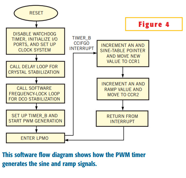
shows the software flow for the DAC. After a reset, the routine stops the watchdog timer, configures the output ports, and sets up the clock system. Next, the software calls a delay to allow the 32,768-Hz crystal to stabilize to calibrate the DCO (digitally controlled oscillator).
Next, the routine calls the calibration routine to set the operating frequency to 2.048 MHz. After the DCO calibration, the program sets up Timer_B, CCR1 and CCR2 for PWM generation and then starts the timer. Finally, the MSP430 goes into low-power mode 0 (LPM0) to conserve power. The CPU wakes up to handle each CCIFG0 interrupt from the PWM timer and then re-enters LPM0. (See references 1, 2, and 3 for more information on the DCO and the MSP430 family.)