http://pdfserv.maximintegrated.com/en/an/AN818.pdf
http://www.maximintegrated.com/app-notes/index.mvp/id/818
Digital Adjustment of DC-DC Converter Output Voltage in Portable Applications
Abstract: This tutorial discusses methods for digitally adjusting the output voltage of a DC-DC converter. The digital adjustment methods are with a digital-to-analog converter (DAC), a trim pot (digital potentiometer), and PWM output of a microprocessor. Each method is assessed and several DACs and digital potentiometers presented.
There are many portable applications that optimize circuit performance by adjusting the output voltageof a DC-DC converter. For instance, many microprocessors can operate at a low voltage to save power, and then operate at a high voltage for increased processing power. Switching between these operating modes requires adjusting the output voltage of a DC-DC converter. Another example is an LCD display; as itstemperature changes, the voltage applied to it must change to maintain the correct contrast ratio.
Adjustments made via digital control have proven to be the most reliable method of performing these and other voltage adjustments. A manual trim pot may be used, but it is often large and can suffer from reliability problems due to wear associated with the manual adjustments; furthermore, it cannot be adjusted under microprocessor control. This article discusses several methods of digitally adjusting the output voltage of a DC-DC converter, with emphasis on devices for portable applications.
Different Digital Method
There are three main methods of digitally adjusting the output voltage of a DC-DC converter:
- A digital-to-analog converter (DAC)
- A trim pot (digital potentiometer)
- A PWM output of a microprocessor (MPU)
DACs
A DAC is simply a digitally-controlled voltage source. The digital interface to a DAC can be either serial or parallel. For applications where the DAC update rate is fairly low (such as DC-DC voltage adjustments), serial interfaces are typically used. They are smaller, using only 2 or 3 wires for aserial interface, compared to 8 to 16 wires for a parallel interface. Fewer pins produce smaller packages, and therefore lowers cost.
The main specifications to consider for a DAC are:
- Supply voltage: 3V or 5V supplies are typically required for portable applications.
- Supply current: low current extends battery life.
- Output voltage swing: the output swing is usually from 0V to VREF (the DAC's reference voltage).
- Number of bits of resolution: The number of bits of resolution determines how many adjustment steps the DAC will have. The number of steps is equal to 2N, where "N" is the number of bits of resolution of the DAC. A 6-bit DAC, for example, will have 26, or 64 steps; while an 8-bit DAC will have 28, or 256 adjustment steps.
Note: The step size at the DAC output is the output voltage swing divided by the number of DAC steps. For example, the MAX5361, a 6-bit DAC with a 4V output voltage swing, has a step size of 62.5mV (4V output voltage swing/26 steps). - Error sources: There are several error sources to consider:
- Full-scale voltage error: For DACs with <= 8-bits of resolution, this error is generally the largest, and will have the greatest effect on overall system accuracy. Low-cost devices can have errors as large as ±25%. However, this initial error can be calibrated out. Calibration usually occurs at production test or the error can be compensated for by using an in-system ADC.
- Offset voltage error: This can also be a large error source, and can be calibrated out if too large.
- Differential nonlinearity (DNL): It is usually necessary that the output of the DAC bemonotonic (i.e., increasing or flat output change for increasing input code). This requires a DNL of ±1 LSB (max).
- Integral nonlinearity (INL): This specification is usually tight enough so as to not be important in these applications.
- Temperature coefficient: The output voltage has a temperature dependence. This error source cannot be calibrated out at production, unless the system is tested over temperature, although it can be calibrated out using an on-board ADC if its temperature drift is low enough. Typically, the temperature drift is small enough so as to not be a problem.
- Internal or external voltage reference: Inexpensive devices with internal references are available. However, if an accurate system reference (i.e., an external reference) is available, it may be used for improved performance.
- Type of interface: serial or parallel. Serial interfaces are required for small size. Typical choices are SPI™, I²C, SMBus™, or bit-banging. Bit-banging entails using general purpose I/O pins to provide the controls necessary for the DAC. The type of interface chosen is a function of the interface(s) supported by the system processor.
- Package size: smaller is better. Very small SOT or SC70 packages are available.
- Volatile or nonvolatile settings: Most DACs have volatile output voltage settings (i.e., they forget their output setting if power is removed). This generally does not pose a problem, since most systems have some sort of nonvolatile memory, which can be used in conjunction with the DAC. Nonvolatile DACs are also available. These devices retain the DAC register setting in on-chip memory so the DAC can "remember" its output setting even if power is removed.

Design Example (Adjustable LCD Output Voltage)
In the circuit of Figure 1, assume that it is desired to have the DC-DC converter's VOUT to be adjustable from a low of VOUT(MIN) to a high of VOUT(MAX).

Figure 1. DC-DC converter with DAC for VOUT adjustment.
The highest DAC output voltage is VDACHIGH. Due to the error sources listed above, there is a tolerance on the VDACHIGH voltage. The higher voltage is VDACHIGH(MAX), and the lower voltage is VDACHIGH(MIN). Similarly, the low output voltage has a low and high voltage limit, VDACLOW(MAX) and a VDACLOW(MIN), respectively.
R1, R2, R3, and the reference all have errors, resulting in the following MIN and MAX variables for these parameters : R1MAX, R1MIN, R2MAX, R2MIN, R3MAX, R3MIN, VREF(MAX), VREF(MIN).
The output voltage of the LCD (VOUT) can be calculated by noting the following:
VOUT = VREF + i1R1 (Eq. 1) i1 = i2 + i3 (Eq. 2) i2 = VREF/R2 (Eq. 3) i3 = (VREF - VDAC)/R3 (Eq. 4)
Substituting Equations 2 through 4 into Equation 1 yields:
VOUT = VREF(1 + (R1/R2)) + (VREF - VDAC) (R1/R3) (Eq. 5)
From Equation 5, it can be seen that the maximum output voltage occurs for the minimum DAC voltage,
and that the minimum output voltage occurs for the maximum DAC voltage.
To ensure that the desired output swing is achieved, choose values of R1, R2, and R3 such that Equations 6 and 7 are met:
VOUTMAX(LOW) = VREFMIN(1 + (R1MIN/R2MAX)) + (VREFMIN - VDACMIN(HIGH))(R1MIN/R3MAX) (Eq. 6) VOUTMIN(HIGH) = VREFMAX(1 + (R1MAX/R2MIN)) + (VREFMAX - VDACMAX(LOW))(R1MAX/R3MIN) (Eq. 7)
Equation 6 refers to VOUTMAX(LOW), instead of just VOUTMAX. Since there are tolerances on the variables on the right hand side of Equation 6, the maximum output voltage also has a tolerance, and can vary from a minimum of VOUTMAX(LOW) to a maximum of VOUTMAX(HIGH). To ensure that the output swings high enough under all possible conditions, Equation 6 refers to the lowest possible voltage of VOUTMAX, namely VOUTMAX(LOW).
Similarly, in Equation 7, the variables all have tolerances, so VOUTMIN can vary from a minimum of VOUTMIN(LOW) to a maximum of VOUTMIN(HIGH). To ensure that the output swings low enough under all possible conditions, Equation 7 refers to the highest possible voltage of VOUTMIN, namely VOUTMIN(HIGH). Note that in Equations 6 and 7, VOUTMAX and VOUTMIN are known values, where VOUTMAX is the maximum desired LCD output voltage, and VOUTMIN is the minimum desired output voltage. The minimum and maximum DAC output voltages (VDACMIN and VDACMAX) can be found in the electrical characteristics table of the DAC being used.
The unknown values are R1, R2, and R3. Since there are three unknowns and only two equations, there is more than one unique solution for the values of R1, R2, and R3. The most straightforward way to select values for R1–R3 is to use a spreadsheet and plug in values for the resistors until Equations 6 and 7 are met. Resistor values should be large enough to prevent excessive power dissipation. A good beginning point is to choose a value for R2 that has been suggested by the manufacturer of the DC-DC converter. Typically, VOUTMAX will be higher than VOUTMAX(LOW), since the latter is calculated using worst-case values. Using the other extreme worst-case values (substituting MIN for MAX, and MAX for MIN, and LOW for HIGH on the right-hand-side of Equation 6) results in the other extreme for VOUTMAX - VOUTMAX(HIGH):
VOUTMAX(HIGH) = VREFMAX(1 + (R1MAX/R2MIN)) + (VREFMAX - VDACMIN(LOW))(R1MAX/R3MIN) (Eq. 8)
(Note: in going from Equation 6 to Equation 8, VDACMIN(HIGH) was changed to VDACMIN(LOW), without changing the "MIN" term to a "MAX" term. This substitution was not made, since Equations 6 and 8 both refer to VOUTMAX, which comes from VDACMIN.)
If VOUTMAX(HIGH) exceeds the maximum voltage rating of the LCD display, the DAC codes which cause the output voltage to exceed the LCD voltage limit must be avoided. For methods on avoiding these codes, see "Compensating for errors in digital adjustment circuitry" below.
Typically, VOUTMIN will be lower than VOUTMIN(HIGH), since the latter is calculated using worst-case values. Using the other extreme worst-case values (i.e., substituting MIN for MAX, and MAX for MIN, and HIGH for LOW on the right-hand-side of Equation 7) results in the other extreme for VOUTMIN, namely VOUTMIN(LOW):
VOUTMIN(LOW) = VREFMIN(1 + (R1MIN/R2MAX)) + (VREFMIN - VDACMAX(HIGH))(R1MIN/R3MAX) (Eq. 9)
(Note: in going from Equation 7 to Equation 9, VDACMAX(HIGH) was changed to VDACMAX(LOW), without changing the "MAX" term to a "MIN" term. This substitution was not made, since Equations 7 and 9 both refer to VOUTMIN, which comes from VDACMAX.)
If VOUTMIN(LOW) is too low for desired operation, the DAC codes which cause the output voltage to go too low must be avoided. For methods on avoiding these codes, see "Compensating for errors in digital adjustment circuitry" below.
Trim Pot
A digital potentiometer is a digitally adjustable resistor. It is generally placed in the feedback loop of a DC-DC converter, and as its value changes, the converter's output voltage changes.
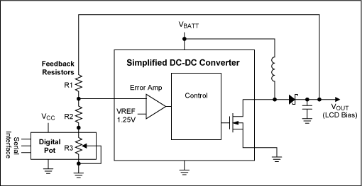
Figure 2. DC-DC converter with digital potentiometer for VOUT adjustment.
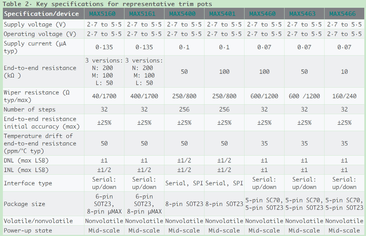
In addition to the important specifications listed for a DAC (supply voltage, supply current, DNL, INL, interface type, package size, volatile/nonvolatile settings), a trim pot adds the following key specifications:
- End-to-end resistance: The potentiometer resistance typically varies from 0Ω to a maximum value given by the "end-to-end resistance" specification in the product data sheet. There is usually a large tolerance for this value (see "Compensating for errors in digital adjustment circuitry" below)
- Wiper resistance: This ultimately determines the lowest resistance value of the potentiometer.
- Operating voltage range: The voltage applied to the high-end, low-end, and wiper of the trim pot must never exceed the operating voltage range of the trim pot
- Number of steps: The steps on a digital potentiometer are typically either linear or logarithmic. For LCD adjustment, a linear adjustment is desired. Dividing the end-to-end resistance by the number of steps determines the step size. For example, the MAX5161NEZT is a 32-step digital potentiometer with 200kΩ end-to-end resistance. Dividing 200kΩ by 32 steps, yields 6.25kΩ per step.
- Error sources:
- End-to-end resistance initial accuracy: This error source is generally the largest, and will have the greatest effect on overall system accuracy. Digital potentiometers can have initial errors as large as ±25%. This initial error must be calibrated out. Calibration usually happens at production test, or an in-system ADC can compensate for it, if one is available. See Figures 4 and 5 and "Compensating for errors in digital adjustment circuitry" below.
- Wiper resistance initial accuracy: This is usually specified very loosely, since the wiper resistance is usually less than the size of one step. This error source can be compensated for using the methods in "Compensating for errors in digital adjustment circuitry" below.
- Temperature Drift of end-to-end resistance: The end-to-end resistance has a temperature dependence. This error source is usually not calibrated out at production, unless the system is tested over temperature. However, if the system ADC is stable enough over temperature, it can be used to compensate for temperature errors. Although, the temperature drift is usually small enough so as to not be a problem.
Design Example
Referring to Figure 2, and using similar naming conventions as in the DAC example, it can be seen by inspection that:
VOUT = VREF × (1 + R1/(R2 + R3)) (Eq. 10)
Note that R3 is the digital potentiometer, and that its value can be changed from R3HIGH to R3LOW. Like the DAC, there are MIN and MAX values for these terms. This results in R3HIGH(MIN) and R3HIGH(MAX), as well as R3LOW(MIN) and R3LOW(MAX). These values can be obtained from the data sheet of the digital potentiometer selected.
Similar values as seen in Equations 6–9 can calculated (see Equations 11–14 below) using the same methodology described above. Certain codes can be avoided by using the methods shown below in "Compensating for errors in digital adjustment circuitry".
VOUTMAX(LOW) = VREFMIN × (1 + R1MIN/(R2MAX + R3LOW(MAX))) (Eq. 11) VOUTMIN(HIGH) = VREFMAX × (1 + R1MAX/(R2MIN + R3HIGH(MIN))) (Eq. 12) VOUTMAX(HIGH) = VREFMAX × (1 + R1MAX/(R2MIN + R3LOW(MIN))) (Eq. 13) VOUTMIN(LOW) = VREFMIN × (1 + R1MIN/(R2MAX + R3HIGH(MAX))) (Eq. 14)
PWM Output
Many microprocessors have PWM outputs. These are digital outputs where the duty cycle of the output is adjusted to change the average output voltage. A "DC" voltage is obtained by placing a low-pass output filter at the PWM output. The duty cycle of a PWM output is the percentage of time the output stays high vs. the period of the PWM output. Many microprocessors allow the selection of both the PWM frequency and the PWM duty cycle. For example, the MC68VZ328 microprocessor provides both a 16-bit and an 8-bit PWM output. The number of bits determines the number of adjustment steps of the PWM output. 8-bits is more than adequate for DC-DC converter voltage adjustment, providing 256 steps of PWM adjustment, from 0% duty cycle to 100% duty cycle.
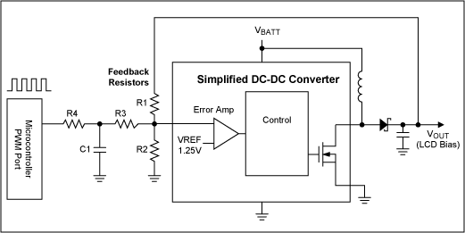
Figure 3. DC-DC converter with PWM for VOUT adjustment.
PWM outputs provide the cheapest method of voltage adjustment, since most microprocessors have at least one PWM output. While inexpensive (since they come with the microprocessor), PWM outputs are costly in terms of power consumption, since they generate a "DC" level by providing a high-frequency output which is subsequently filtered. The high-frequency switching of the PWM output stage consumes much more power than a low-power DAC or digital trim pot, both of which are DC by nature. In Figure 3, filtering of the PWM AC waveform is provided by the R4-C1 combination. R3 is used to isolate C1 from affecting the AC performance of the R1-R2 feedback loop.
PWM outputs are by nature inaccurate, since their output voltages are a function of the digital levels VOH and VOL. Because VOH and VOL are digital output voltage specifications, they are specified very loosely (VOH can be anywhere between VOH min and VCC, the I/O supply to the microprocessor; and VOL can be anywhere between VOL max and GND). And, since these digital levels are typically a function of VCC, they vary as the supply voltage to the processor varies.
The important specifications for a PWM output are:
- VOH and VOL: The specified levels (or ranges) for each, along with the duty cycle determine the nominal (DC) output voltage of the PWM output.
- Duty cycle: both range and accuracy are important. The duty cycle determines what percentage of the time the output will be at VOH, and what percentage it will be at VOL.
- PWM frequency: The frequency is important, since to be useful, the PWM output must be filtered by a low-pass filter. The PWM frequency is used to calculate the attenuation of the PWM ripple (the PWM output swings from VOH to VOL, and to be useful for adjusting a DC-DC converter output, this AC square-wave must be converted to a low-ripple "DC" signal).
Since VOL and VOH are specified so loosely, PWM outputs are really best used in closed-loop systems such as LCD control or audio volume control, where the absolute accuracy isn't important. In these cases, the user simply increases or decreases the voltage as necessary. However, with the inaccuracies posed by the PWM outputs, some measurement must be made to ensure that the PWM signal never causes a high enough output voltage to cause damage to other circuitry. This measurement can be done at production test, by measuring the output voltage of the PWM over certain parameters (temperature, loading of the power supply, etc.). Alternatively, it can be accomplished by measuring the LCD output voltage with an ADC, and keeping the LCD voltage within range via software (see "Compensating for errors in digital adjustment circuitry" below).
Design Example
Referring to Figures 3 and 1, and using the similar naming conventions as in the DAC example, the output voltage (VOUT) can be calculated by making the following substitutions into Equation 5: substitute R3 + R4 for R3; and substitute VPWM = D × VOH + (1 - D) × VOL for VDAC. VPWM is the average output voltage of the PWM, D is the duty cycle of the PWM (in %), VOH is the output voltage high voltage, and VOL is the output low voltage.
VOUT = VREF(1 + (R1/R2)) + (VREF - D × VOH + (1 - D) × VOL)(R1/(R3 + R4)) (Eq. 15)
Note that the value of D can be changed from DHIGH to DLOW (typically 100% to 0%, in discrete increments). The duty cycle has tolerance (although it is typically not specified in the processor data sheet), which leads to DHIGH(MAX), DHIGH(MIN), DLOW(MAX), and DLOW(MIN). The digital output voltages VOH and VOL also have tolerances, which lead to VOH(MIN), VOH(MAX), VOL(MIN), and VOL(MAX).
The same values as in Equations 6–9 can be calculated (see Equations 16–19 below). The duty cycle values which would cause the output voltage to exceed the maximum desired voltage (similar to the digital codes for a DAC or trim pot) can be avoided using the methods shown below in "Compensating for errors in digital adjustment circuitry".
VOUTMAX(LOW) = VREFMIN(1 + (R1MIN/R2MAX)) + (VREFMIN - DLOW(MAX) × VOH(MIN) + (1 - DLOW(MAX)) × VOL(MIN))(R1MIN/(R3 + R4)MAX) (Eq. 16) VOUTMIN(HIGH) = VREFMAX(1 + (R1MAX/R2MIN)) + (VREFMAX - DHIGH(MIN) × VOH(MAX) + (1 - DHIGH(MIN)) × VOL(MAX))(R1MAX/(R3 + R4)MIN) (Eq. 17) VOUTMAX(HIGH) = VREFMAX(1 + (R1MAX/R2MIN)) + (VREFMAX - DLOW(MIN) × VOH(MAX) + (1 - DLOW(MIN)) × VOL(MAX))(R1MAX/(R3 + R4)MIN) (Eq. 18) VOUTMIN(LOW) = VREFMIN(1 + (R1MIN/R2MAX)) + (VREFMIN - DHIGH(MAX) × VOH(MIN) + (1 - DHIGH(MAX)) × VOL(MIN))(R1MIN/(R3 + R4)MAX) (Eq. 19)
Compensating for Errors in Digital Adjustment Circuitry
There are two common methods for overcoming the inaccuracies of the digital circuitry used to adjust the DC-DC converter (see Figures 4 and 5). Both involve measuring the output voltage of the DC-DC converter using an ADC, and using that measurement (or measurements) to compensate for the initial errors of the digital adjustment circuitry, and of the DC-DC converter.
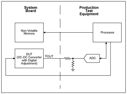
Figure 4. Measuring error of DC-DC converter and digital adjustment circuitry at production test.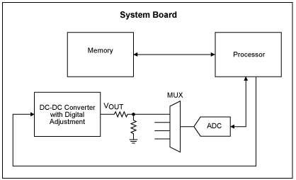
Figure 5. Measuring output of DC-DC converter and digital adjustment circuitry with on-board ADC.
One method uses the ADC on the system board (Figure 4), while the other uses the ADC on a piece of production test equipment (Figure 5). Each method has its own advantages and disadvantages.
The benefit of using the ADC on the system board is that it does not require a separate step at production test. Additionally, if the ADC is accurate over temperature, it can compensate for temperature drift errors inherent in the digital adjustment circuitry and in the DC-DC converter. Using the system ADC, however, requires that the on-board ADC be sufficiently accurate, and that it have a spare channel.
There are two common methods employed when using an ADC on the system board. The first entails measuring the DC-DC converter's output voltage every time the output code is changed. By monitoring the output voltage, one can avoid codes that would result in output voltages outside of the desired range.
The second method requires measurement of the DC-DC converter's output, typically when power is first applied to the device. The output voltage is measured with several different codes applied, allowing one to determine the initial errors such as offset and full-scale error (for an ADC), full-scale resistance (for a trim pot), or VOH and VOL (for a PWM signal). With knowledge of these initial errors, an algorithm can be used to avoid those codes that would result in output voltages outside the desired range.
When production test equipment is used to measure the errors of the adjustment circuitry and the DC-DC converter, the second compensation method (above) should be applied. A benefit of using production test equipment is that this method does not require a system ADC. Additionally, the measurement circuitry on the test equipment can be very expensive (and accurate, precise, etc.) without significantly increasing the cost of the end product, since its cost is spread out over the lifetime of the test equipment, whereas the cost of the system-board's ADC is built into each unit. And, if the devices are tested over temperature, temperature errors could also be eliminated. But testing over temperature is typically too expensive, and is usually not needed.
Overvoltage Issues
Many DACs power up to zero-scale, which causes VOUT to be at its maximum value, as seen in the application circuit of Figure 1 (see Equation 5). If VOUTMAX(HIGH) (Equation 8) exceeds the operating voltage range of the LCD supply, the DAC output must be raised to a value that does not allow the output of the DC-DC converter to get too high, before the DC-DC converter has powered up. One method of doing this is to keep the DC-DC converter powered off until the DAC output has been adjusted. Another method is to select a DAC that powers up to mid-scale, so that overvoltage issues are not a problem.
Similarly, for the PWM, make sure that its output is not set to zero with the LCD DC-DC converter powered-up; such a condition can cause VOUTMAX(HIGH) to exceed the limitations of the LCD device (see Figure 3 and Equation 18).
Many digital potentiometers power up to half-scale, which is a benign state for DC-DC converter adjustment. However, if powering up to half-scale causes VOUTMAX(HIGH) to exceed the limitations of the LCD device (see Figure 2 and Equation 13), then the DC-DC converter must be kept off until the potentiometer is set to a higher value.