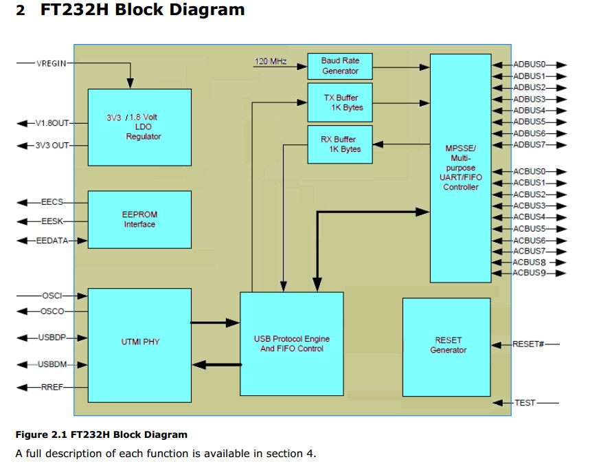
FT232H不仅支持异步串行接口(UART),还通过其内建的多协议同步串行引擎(MPSSE)支持许多同步IO接口,比如SPI, I2C,JTAG以及FPGA编程接口,MPSSE通信速度能够达到30M比特/秒。另外,MPSSE可用于执行设计工程师自己的同步串行总线协议。
新的FT1248 总线是FT232H集成的一个接口功能,为专有的同步半双工串行/并行接口,与外部逻辑通信速率可以达到30M Byte/秒。FT1248 总线独特之处在于能够根据可用物理数据总线的数量(1,2,4或8)调整FT232H与外部逻辑连接的带宽, 从而为系统设计提供最优的适应性。
集成的1.8V和3.3V低压差稳压器减少了所需外部元件,同时与现有的USB2.0兼容的全速产品相比较而言,1 K字节大的收发数据缓存加上USB2.0高速技术大大改善了数据吞吐量, 缩减了延迟响应时间。FTDI网站可下载用于Windows, Linux, MAC 和 WinCE操作系统的免税驱动。
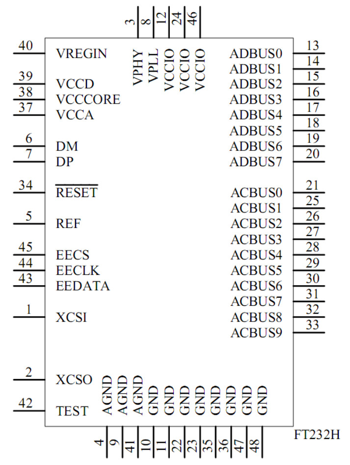
FT232H的封装选择有48针LQFP(FT232HL)或48针QFN(FT232HQ)无铅封装。这两种FT232H工作范围是-40⁰C ~ +85⁰C。FT232HL定价为$2.75(1,000片以上),FT232HQ定价为$2.60(1000片以上)。UM232H用户评估模块有助于快速建立原型或测试FT232H平台,与一个标准的0.6英寸宽,28针的DIP插座连接。UM232H模块单价定为$20(1~9片)。
Operating at USB Hi-Speed 480Mbps rate, this fast single channel bridge chip features either a flexible serial interface or parallel FIFO interface, with data transfer speeds up to 40Mbytes/s. Using a serial EEPROM interface, this device can be configured for a wide variety of asynchronous and synchronous serial standards, such as JTAG, SPI, I2C and UART as well as synchronous and asynchronous parallel FIFO interfaces. In addition, this device features the new synchronous, half-duplex FT1248 bus, which allows an engineer to trade off bandwidth for pin count using 1, 2, 4, or 8 data lines at up to 30Mbytes/s. The I/O structure is 3.3V with built-in tolerance for 5V, allowing the designer maximum flexibility when interfacing with FPGAs. On-board voltage regulation provides 3.3V and 1.8V supplies from a 5V source, as well as a power-on-reset function. FTDI provides royalty-free virtual com port and D2XX drivers for Microsoft Windows (XP – Windows7), Apple Mac OSX, and Linux. This 48 pin device is available in either LQFP or QFN packaging, and is ROHS compliant.
- Single channel USB to serial / parallel ports with a variety of configurations.
- Entire USB protocol handled on the chip. No USB specific firmware programming required.
- USB 2.0 Hi-Speed (480Mbits/Second) and Full Speed (12Mbits/Second) compatible.
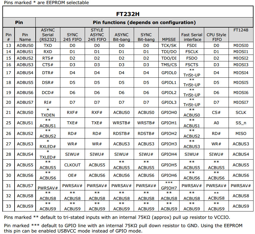
- Multi-Protocol Synchronous Serial Engine (MPSSE) to simplify synchronous serial protocol (USB to JTAG, I2C, SPI or bit-bang) design.
- UART transfer data rate up to 12Mbaud. (RS232 Data Rate limited by external level shifter).
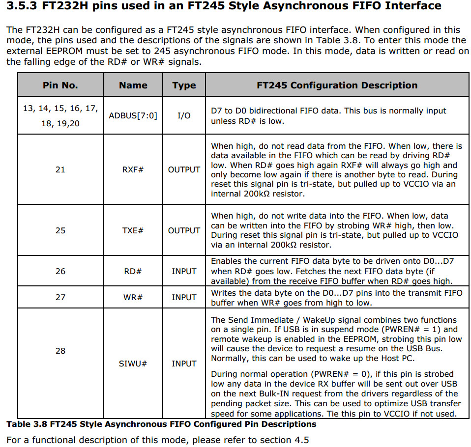
- USB to asynchronous 245 FIFO mode for transfer data rate up to 8 MByte/Sec.
- USB to synchronous 245 parallel FIFO mode for transfers up to 40 Mbytes/Sec
- Supports a half duplex FT1248 interface with a configurable width, bi-directional data bus (1, 2, 4 or 8 bits wide).
- CPU-style FIFO interface mode simplifies CPU interface design.
- Fast serial interface option.
- FTDI's royalty-free Virtual Com Port (VCP) and Direct (D2XX) drivers eliminate the requirement for USB driver development in most cases.
- Adjustable receive buffer timeout.
- Option for transmit and receive LED drive signals.
- Bit-bang Mode interface option with RD# and WR strobes
- Highly integrated design includes 5V to 3.3/+1.8V LDO regulator for VCORE, integrated POR function
- Asynchronous serial UART interface option with full hardware handshaking and modem interface signals.
- Fully assisted hardware or X-On / X-Off software handshaking.
- UART Interface supports 7/8 bit data, 1/2 stop bits, and Odd/Even/Mark/Space/No Parity.
- Auto-transmit enable control for RS485 serial applications using TXDEN pin.
- Operation configuration mode and USB Description strings configurable in external EEPROM over the USB interface.
- Configurable I/O drives strength (4, 8, 12 or 16mA) and slew rate.
- Low operating and USB suspend current.
- Supports self powered, bus powered and high-power bus powered USB configurations.
- UHCI/OHCI/EHCI host controller compatible.#
- USB Bulk data transfer mode (512 byte packets in Hi-Speed mode).
- +1.8V (chip core) and +3.3V I/O interfacing (+5V Tolerant).
- Extended -40°C to 85°C industrial operating temperature range.
- Compact 48-pin Lead Free LQFP or QFN package
- Configurable ACBUS I/O pins.

This mode uses a synchronous interface to get high data transfer speeds. The chip drives a 60 MHz CLKOUT clock for the external system to use.
Note that Asynchronous FIFO mode must be selected in the EEPROM before selecting the Synchronous FIFO mode in software.
4.4.1 FT245 Synchronous FIFO Read Operation
A read operation is started when the chip drives RXF# low. The external system can then drive OE# low to turn the data bus drivers around before acknowledging the data with the RD# signal going low. The first data byte is on the bus after OE# is low. The external system can burst the data out of the chip by keeping RD# low or it can insert wait states in the RD# signal. If there is more data to be read it will change on the clock following RD# sampled low. Once all the data has been consumed, the chip will drive RXF# high. Any data that appears on the data bus, after RXF# is high, is invalid and should be ignored.
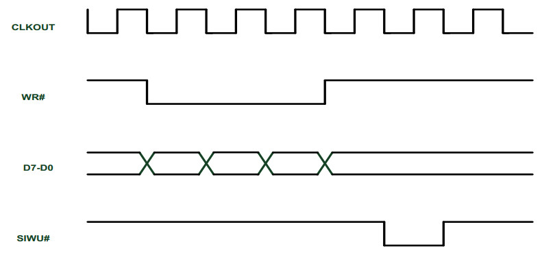
4.4.2 FT245 Synchronous FIFO Write Operation
A write operation can be started when TXE# is low. WR# is brought low when the data is valid. A burst operation can be done on every clock providing TXE# is still low. The external system must monitor TXE# and its own WR# to check that data has been accepted. Both TXE# and WR# must be low for data to be accepted.
4.12 Send Immediate / Wake Up (SIWU#)
The SIWU# pin is available in the FIFO modes and in bit bang mode.
The Send Immediate portion is used to flush data from the chip back to the PC. This can be used to force
short packets of data back to the PC without waiting for the latency timer to expire.
To avoid overrunning, this mechanism should only be used when a process of sending data to the chip
has been stopped.
The data transfer is flagged to the USB host by the falling edge of the SIWU# signal. The USB host will
schedule the data transfer on the next USB packet.
Figure 4.25: Using SIWU#
When the pin is being used for a Wake Up function to wake up a sleeping PC a 20ms negative pulse on
this pin is required. When the pin is used to immediately flush the buffer (Send Immediate) a 250ns
negative pulse on this pin is required.
Notes
1. When using remote wake-up, ensure the resistors are pulled-up in suspend. Also ensure peripheral
designs do not allow any current sink paths that may partially power the peripheral.
2. If remote wake-up is enabled, a peripheral is allowed to draw up to 2.5mA in suspend. If remote
wake-up is disabled, the peripheral must draw no more than 500uA in suspend.
3. If a Pull-down is enabled, the FT232H will not wake up from suspend when using SIWU#
4.In UART mode the RI# pin acts as the wake up pin.