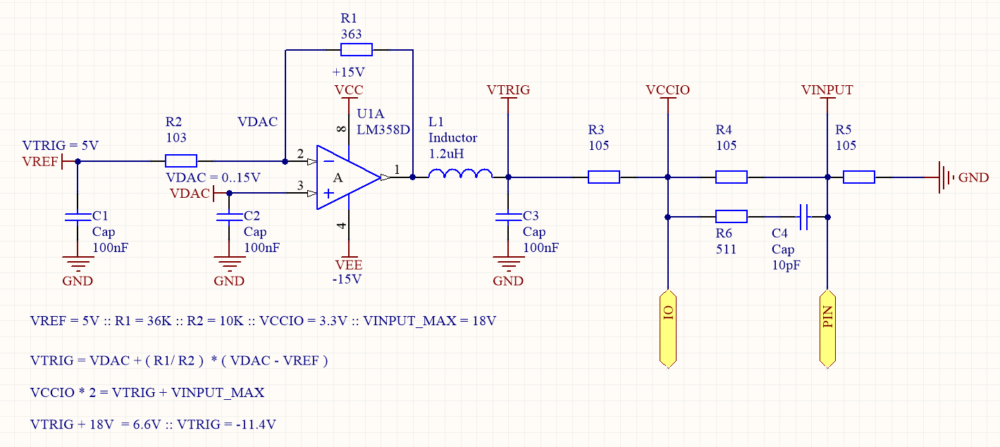
Voltage Translation for Analog to Digital Interface ADC
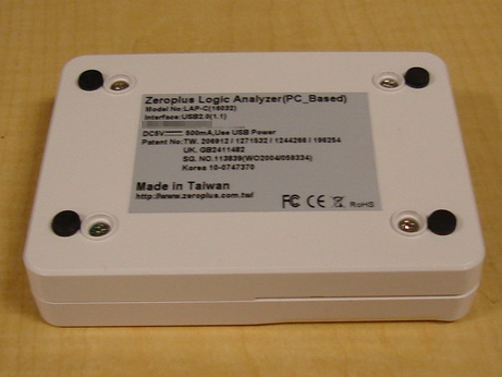
http://openschemes.com/2010/03/23/zeroplus-logic-cube-review-and-teardown/

LAP 16032 has 4.5MBIT SRAM and can aquire up to 128k per chn, now my LAP 16032 has 18MBIT SRAM
The device scores high marks on our chart for:
- Dependability - You plug it in, and it does what it says it’s going to. No screwing around with dodgy drivers and flaky hardware. These guys really do seem to use their own hardware, and it shows. FEBE? For engineers, by engineers?
- Reliability - It always does what it says it’s going to do. It doesn’t miss edges or do other stupid stuff. Ever, as far as we can tell and that’s a big plus for us.
- Portability - It’s nice that the whole setup: Cube, USB cable, fancy colored wires, and some minigrabbers all fit nicely in a ziplock bag. Keeps it fresh, as well.
- Capability - Depending on how much money you’re willing to spend, you can get a device with 16 or 32 channels, and memory ranging from 32k to 2MB. That’s a lotta sampling! But since these guys aren’t stupid, they added some pretty awesome triggering and compression that gives you tons of sampling with very little memory. Also, the plug-in protocol analyzers are fantastic. We hate counting I2C clocks and writing hex characters by hand, so having the software do all the work is great.
- Hackability - Due to economies of scale naturally found in manufacturing, the board we got (smallest mem, lowest channels) was able to be upgraded to a pretty awesome box for just about $10. Oh, that and a shitload of work. But that stuff’s considered fun over here.
Teardown & Functional Description
Teardown is dead freakin easy. Remove the 4 rubber feet on the bottom/back to reveal 4 totally goofy sheet-metal looking screws. The only part of the device that was oddly low-quality was these screws. Not a big deal, but when you open and close the box about a thousand times, you think how ugly they are about a thousand times. Guess it stuck.
LAP-C is what they call it, so that’s what we’ll be calling it too. Guess it’s the lower-end of what ZeroPlus manufactures, but it’s fine for us. Blows SUMP clean out of the water, and trust us – we love SUMP! But you get what you pay for, really.
One thing you’ll notice is that we’re blurring out the device’s serial number. Why? Well when we went googling, we found that all the serial numbers were always blurred out. It occurred to us that the image of a serial number must be considered pornographic in Taiwan, so we decided to blur ours in order to show respect.
Sure, the protocol licensing is tied to the serial number among other things, but unless we showed our serial number AND our license key, AND you changed your device’s serial number to ours – we can see no way that the public viewing of a serial number could in any way affect ZP. But still blurred – and hence, they must either be highly offensive or highly arousing and in either case are not suitable for public viewing.
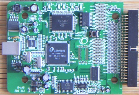
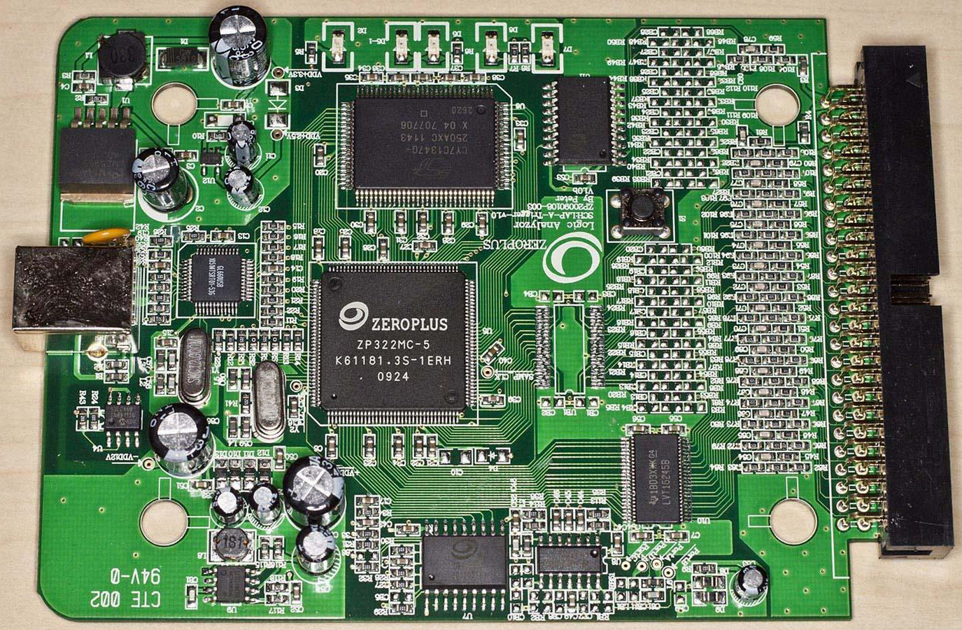
Once you’ve gotten the case off, you can see the LAP-C is a single-board device centered around a big old custom ASIC. We’re not sure if it’s truly custom but since there’s no platform flash nearby it’s not a repackaged Xilinx. Anyway, we trust ZP to be able to make an ASIC and have no need to decap this one, so this chip stays unmolested.
As we said before, we bought the cheapest one (LAPC 16032, 16 channel, 32k RAM) in hopes that we could hack it up. Keep that in mind when reviewing the pix.
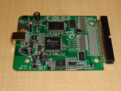
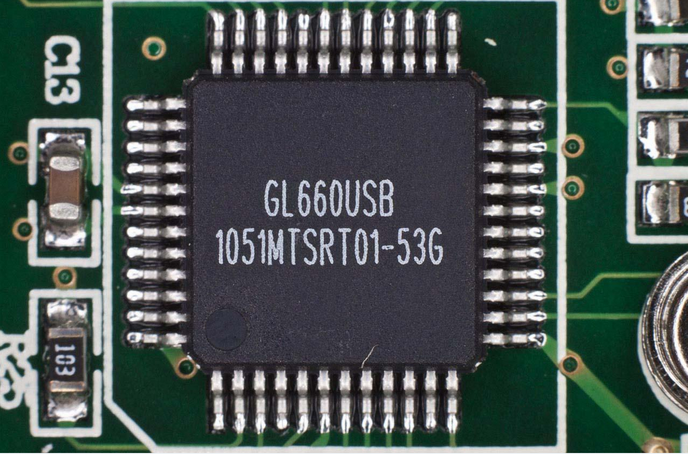
We’ll give a quick rundown of the operation. USB comes in on a Genesys Logic GL-660 old-school USB->IEEE1284 controller, which must have been a legacy design as the 660 is all but dead as far as we can tell. Here’s a GL-660USB Datasheet that really gives very little information. We’re trying to determine if the 660 can write his own serial eeprom over USB, so if you know either way – plz contact us!
The GL660 interfaces directly to the ASIC, so let’s go there next. It’s a ZeroPlus custom as we said before, marked ZP322MB-5. Let’s inspect that again. ZP 32 2MB -5. Uh, looks like our chip is actually a 32 channel, 2MB RAM device. Well that’s the top of the line analyzer there, buddy. How’d we get that top-of-the-line chip in our crappy little 16032?
Economies of scale! It’s way cheaper to make two of the same chip than one each of two types, so the standard practice is to make one full-featured IC and disable features for the peons who can’t afford those features. It’s great for the manufacturer, and the loss due to nerds like us hacking in those missing features is still less than the cost of running two sets of wafers. Now is that a bad thing to do? Are we subverting something we shouldn’t? What are the ethics of “hacking in” features.
We think of it like this: If you buy a Honda Civic, nobody would think twice about you ripping open the engine and installing a turbo or something. Now you’ve added $5k to the value of the car for the few hundred bucks the turbo hardware would cost. It’s the same thing here – we’re like mechanics for electronics. We have the expertise, and enjoy the challenge so we will add, subtract, cut, patch, solder, and reflash whatever we can in order to soup up our toys..
So we know the main IC probably has the capability to do more than what the label says. Let’s keep going. The RAM chip just north of the ASIC is a Cypress CY7C1347G, which is a 4Mbit (128k x 36) pipelined synchronous ram (that means fast, and does stuff on clock edge only in order to be fast). We make the guess that the width of 36 is probably used for 32 channels, so our installed RAM is 128k, not 32k!
That’s kind of weird – economies of scale don’t really apply to things like RAM because the “feature” is directly proportional to die size. Cutting the ram in half requires just over half the silicon (fixed overhead for address decoder and sense amps, but half the cells) so the cost is nearly linear. Cypress must have a SIGNIFICANT volume discount for buying multiple chips of one type instead of fewer chips of multiple types. In other words – Cypress is gouging the small customers, and it’s cheaper to buy 128k and disable most of it than it is to buy a smaller RAM chip. Our guess is due to the fixed package cost outweighing the silicon cost.
Good for us because we have a nice big chunk of memory on hand, and a master processor that can handle it. Just in case you’re wondering – Replacing the 128k chip with a 2M chip is insanity without a hot air rework station, so don’t get greedy and start thinking that you can get the 322000 in a simple hack. But a something-128 might be possible.. ![]()
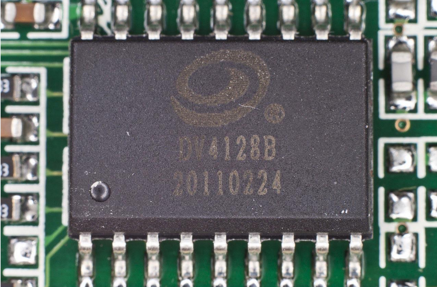
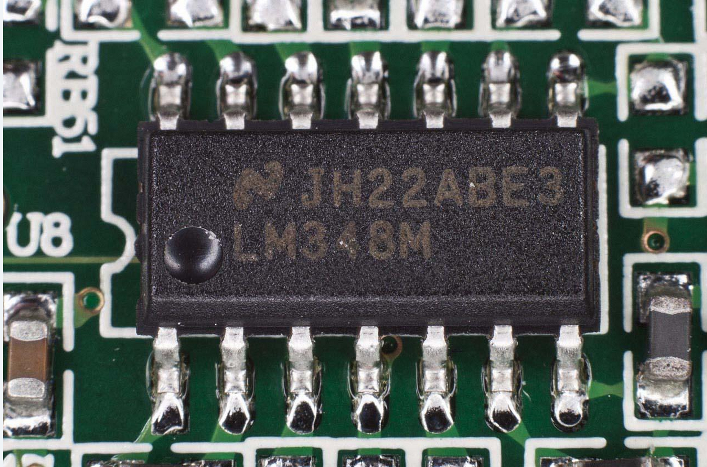
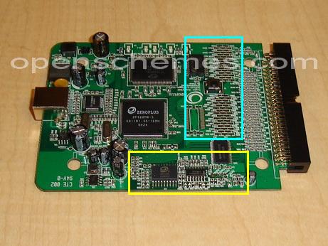
All the way south on the PCB sits another ZeroPlus custom chip (DV4128B) and an LM348 quad 741 op-amp. The ZP chip is a 3.3v Serial DAC, and with the op-amps is used to generate buffer voltages to adjust the trigger points for each of the 4 “ports”, where one port is 8 bits or 8 logic analyzer inputs. We really liked the clever design of the buffer, whereby adjusting the voltage at the top of a resistor divider sets up a fixed 1.67v trigger so a super cheap 74xx series buffer can be used as combination input level shifter and logic buffer. More on that in a future article.
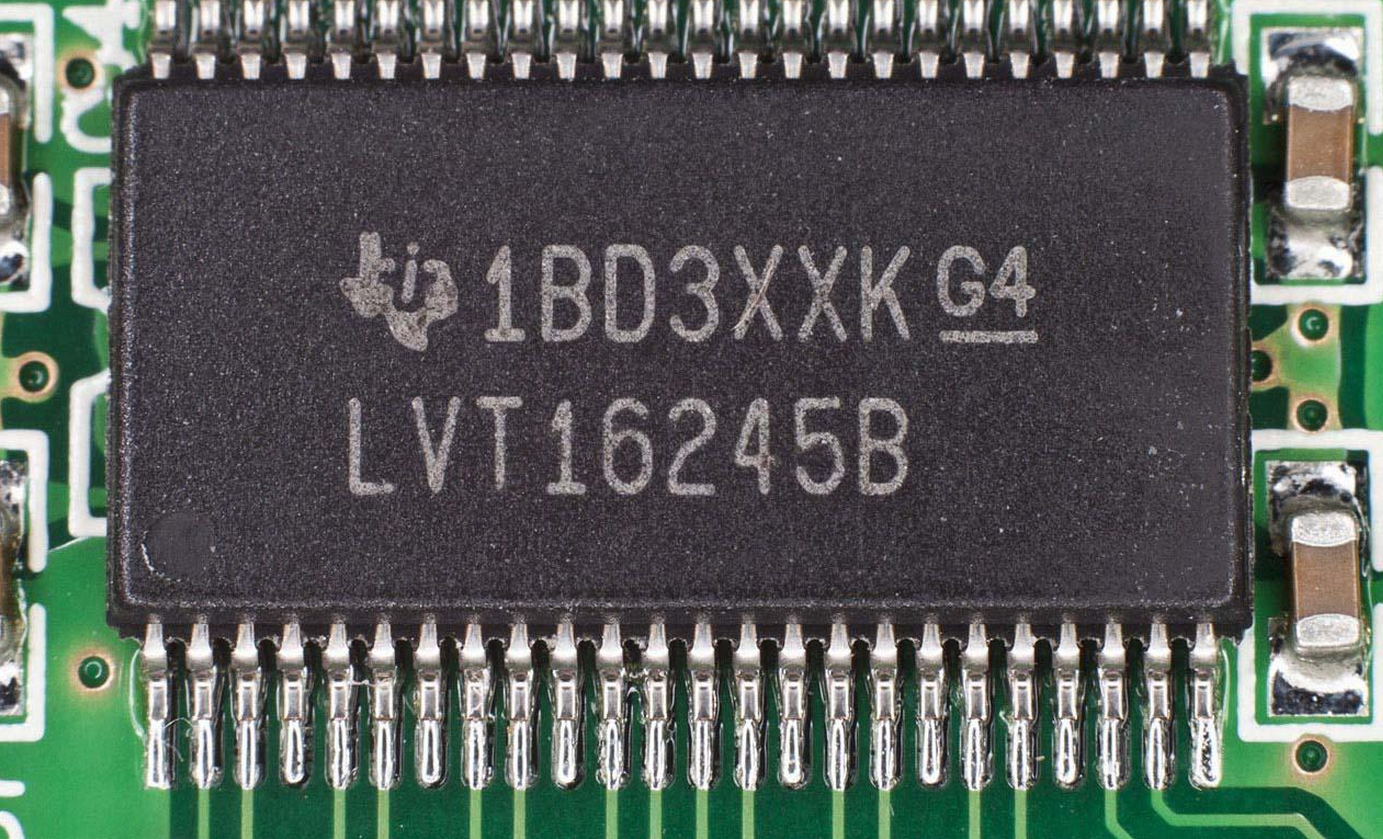
And last but not least, we have the 74LVT16245B 16-channel transceiver and it’s accompanying 16 R divider+RC arrays that is used in conjunction with the buffer voltage to translate various input levels to a fixed 3.3v logic level for the ASIC. Again, this is a really elegant design and we’re glad to have been able to see it – Thanks, ZP!
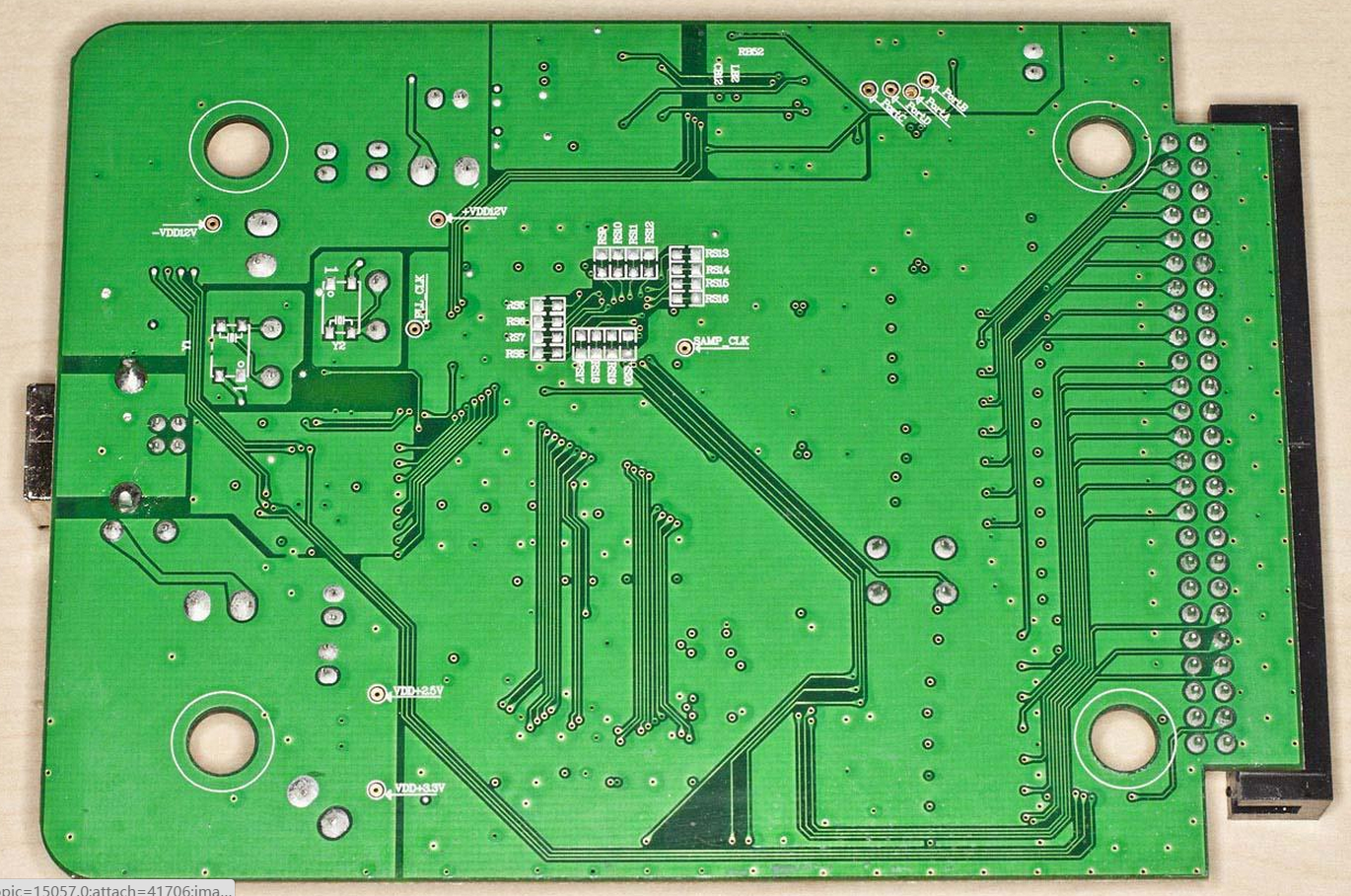
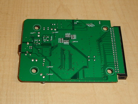
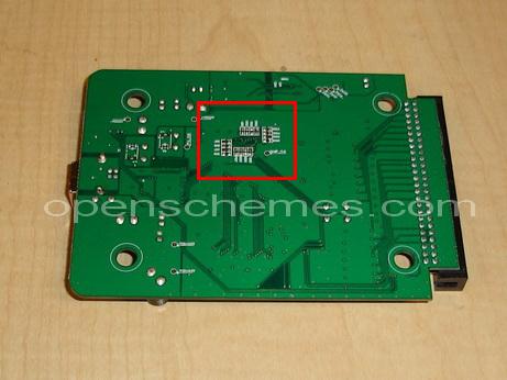
Now you can take a look at the back of the board, which is mostly ground plane and routing except for 16 empty resistor padstacks for the unused channels that have inherent shorts to ground. Guess it’s cheaper to draw a pcb trace than to pull the unused channels to GND with a resistor. No argument there!
We’d better end the article here before we end up giving away too many secrets, but be sure to stay tuned for the next installment where we get buck nasty with the LAP-C.
As always, thanks for taking this little walk with us through a very cool device. We hope your brains are already buzzing with ideas on possible hacks.
For those who’d like a higher-res photo of the front of the PCB, you can get it below or search around on the interwebs for some other really nice teardown pix.

http://openschemes.com/2010/03/27/zeroplus-logic-cube-the-modification/
You may have read in our last article that we’ve been digging around in the Logic Cube and found that, in a hardware sense, it’s an easy mod to install the other 32 channels. And of course, we pointed out that the RAM installed on our board was a 128K, not a 32k. So it seems that with a minimum of work, we can upgrade our $120 16032 to a 32128 which would have cost us a few hundred bucks more.
As gedesu mentioned in a comment, the famed bushing already discussed this hack a few months ago on a hardware forum page. Sadly, we never saw this page and I suppose we’ve gone and duplicated efforts a bit as we developed our mod independently. But we were actually able to catch bushing and a few other developers for a few minutes today and had a very nice discussion on modding the device. Seems both they and we had discovered a few secrets that the other hadn’t, and a lively exchange took place.
The mod really is as simple as installing the missing channels and trigger buffer circuitry. Now when we say simple, we mean simple for a person that is pretty skilled in soldering. This is not a project for a first time user, as the risk of damaging the device would be high. But if you’re careful and thoroughly check the connections before powering up, you should be fine.
The total cost is less than $5 in parts. We bought everything but the 74LVT16245 from HSC, so the prices listed are what we paid. We bought the 74LVT16245′s from Mouser because they don’t gouge like Digi-Key or Arrow.
Here’s what you will need:
- 1x 74LVT16245B 3-state Bus Transceiver ($0.56) – You need to get the DGG (“74LVT16245BDGG”, 48-TSSOP) package. We couldn’t find the TI part and got an NXP LVT16245 as well as a 74ABT16245. We ended up using the ABT chip but the LVT is probably the better choice. Hereafter will be called the ’245.
NOTE: the NXP 74LVT16245B is NOT SUITABLE for this mod. It latches up when an external signal is applied. Our suspicion is the 10pF cap in the input circuit drives the input pin a little beyond the rail and NXP did not account for this in their circuit. Amateur mistake! Especially when cloning a chip that has been around for what, 15 years, with no latchup issues. Booo! Credit for this catch goes to Jake, who traced the problem back and raised the issues when we failed to mention the latchup and just switched to the ABT without telling you valuable readers why it was done. Apologies!
- 1x NXP 74ABT16245B or genuine TI 16LVT245B. These are two chips that are verified not to latch up in the application. Both come in the DGG package.
- 48x 1MEG SMT resistors (48x $0.02) – 0603 package is good and not too tiny. You need 3 for each channel you’re adding, so get 55 or so. They always land upside down when you dump them out of the tape & reel and the natural inclination is to press one side to get it to flip neatly over. But sometimes that ends up in your resistor shooting off somewhere never to be found. Getting extras of all the SMT components is probably a good idea.
- 16x 510 Ohm SMT Resistors (16x $0.02) – Again, we used 0603 size. One for each channel you’re adding. Get extras.
- 16 10pF SMT Capacitors (16x $0.05) – One for each channel. 0603 if you can find them, otherwise 0402. Get extras.
- 2x 10k SMT Resistors (2x $0.02)- One for each of the two new trigger buffers (each buffer drives 8 lines. eg: C0-C7 and D0-D7)
- 2x 36k SMT Resistors (2x $0.02)- One for each of the two new buffers.
- 8x 120nF SMT Capacitors (8x $0.05)- Two each for each of the two new buffers, and 4 for the decoupling caps of the ’245. 0.1uF is probably fine as well.
- 2x 1.2uH SMT Inductors (2x $0.07)- One for each of the two new buffers. Debatable. We lost ours and used wire to short these pads, but we’re very willing to debug the PCB if noise issues arise. If you don’t want to mess around, install them.
- 2x 12pF SMT Capacitors (2x $0.05)- One for each of the two new buffers. You can probably use a 10pF if you just want to buy more of those from above.
- Fine Point Tweezers – For holding the SMT components.
- Fine Point Soldering Iron – The tip should be pretty small to solder the leads of the ’245 accurately. Similar to a toothpick tip if you can find it. We’ll give you a technique to make ithe TSSOP soldering as easy as possible, but a fat tipped soldering iron still won’t work. Get a fine point tip before starting.
- Thin Solder – that 10 gauge crap for pipes ain’t going to cut it. That stuff would be acid core anyway and will eventually eat away your PCB so don’t even consider it. Invest the $30 in a spool of nice fine rosin core solder. Thinner than 0.8mm would be great. Our spool has lasted 5 years or more and we solder like mad bastards, so the initial investment can be amortized over many projects.
- Liquid Solder Flux – Try to get a “flux pen”, but the brush-on stuff should also be fine. You’ll paint the leads of the 16245 when soldering to hopefully lessen the chances of solder bridges. You can also paint the pads of the RC networks if you’re having trouble with solder slop. Flux is awesome like that – it makes solder want to stick to metal and not want to stick anywhere else. So your solder will jump right on the pad and won’t slop around. If you don’t use it – get it. Cleans up with Ethyl Acetate (Flux cleaner) or Acetone and a cotton swab.
- Solder Wick/Braid – A loosly braided mass of thin copper wires soaked in flux. It sucks up solder in order to desolder components or clean up bridges and blobs. To tell the truth, desoldering usually requires MORE solder so the thermal intertia keeps it liquid long enough for you to pull off the part. But then you still need the braid to get those little puddles of solder off your PCB and device.
OK, got all your stuff? Are you ready to start the build? Continue on, intrepid reader!
Overview of the LAP-C Modifications
Below is the overview of the areas we’re going to work in. We have 3 main sections where we will be doing mods.
- Input Circuit (BLUE) – One for each channel. Starts with 3 1M resistors in a resistor divider chain. Across the middle resistor is a series connection of a 510 Ohm resistor and 10pF cap. The external port connects to the 510 Ohm side of this network, and the ’245 input connects to the 10pF capacitor side.
- Trigger Voltage Buffers (YELLOW) – An interesting circuit that uses an opamp to generate a dac-controlled voltage for each port (set of 8 channels). This trigger buffer voltage is fed to the top of all 8 resistor divider chains in the input circuit. By varying the buffer voltage, the device adjusts various input levels up or down to match the input threshold of the 3.3v ’245.
- Unused Channel Shorts (RED) – On the back of the board are 16 empty resistor padstacks. In the center of these are a small trace shorting the pads together. This is shorting the 16 unused channels to GND. You’ll need to carefully cut the shorting trace without gouging too deep into the board. We used a tiny flathead screwdriver tip to gouge a channel which worked fine.
Build Details I – Input Circuit
The input circuit consists of one RC network for each of the 16 channels
we are adding and one 74LVT16245B IC to get data from those 16 channels.
Installing all the components for 16 RCR networks is tedious, but simple work.
Installing the ’245 is tricky and requires a steady hand.
But you’ll have lots of soldering practice with the RCR networks to get you warmed up for the ’245!
The RC network consists of 3x 1MEG resistors, plus a 510 Ohm and a 10pF cap.
We will call these R1-R3, R4, and C1 respectively.
They will be named differently on the board of course, these names are just for illustration purposes.
First, let’s look at the schematic view of the RC network.

Fig 3 – Schematic View of the Input Circuit
We cheated and made the schematic look exactly like the layout, hope you don’t mind.
The operation of the input circuit is as follows:
The resistor divider from Vtrig to GND sets up a 2/3 Vtrig and a 1/3 Vtrig at it’s two center nodes.
For a floating pin, the ’245 sees 2/3 Vtrig which should be out of the way if ZP did their math.
If the pin is pulled high or low, the trigger divider acts to also divide down the pin voltage
in order to keep the input to the ’245 in the 3.3v range.
Great stuff, very clever work.
The 10pF is a fast path to ram a nice sharp edge into the ’245 when the pin changes state,
because sending that signal meandering through a 1MEG will really soften it up.
At this point, you should easily recognize the layout view as seen over and over on the PCB in Section 1.
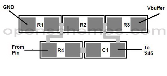
Fig 4 – Layout View of the Input Circuit
In order to solder all these components, we suggest you get an assembly line going and do all the 1MEG,
then all the 510 Ohm, and then all the caps.
It’s much easier and less error prone than having several little piles of SMT components and trying to grab one of each.
The biggest pain in soldering SMT’s is the situation where you have solder on both pads and want to melt it all at once – it doesn’t work.
One side always cools and you’re stuck tapping back and forth with the iron.
You’ll end up overheating the PCB and peeling traces, which really sucks and can ruin your board.
Your strategy should be to get in, get the part mounted well, and get out quickly.
We suggest soldering one side of each component at a time, and even cleaning off the other pad using solder wick
if it already had solder on it or accidentally gets some solder on it.
That way, you don’t have to deal with the case of trying to heat two pads at once.
We’ll break our soldering technique down into three steps that fit with our assembly line analogy.
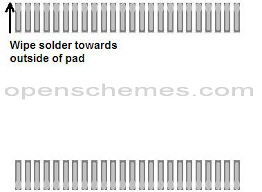
Step 1 – Put a small blob of solder onto each of the right hand pads. Or the left hand pads if if you’re a lefty.
You’re going to be holding the iron in your good hand and tweezering in components with your other hand.
In order to avoid having to cross over, simply blob the side you’d naturally have the iron in.
You want a small blob – not a pinprick, and not a huge overflowing mass.
Our pic here is actually showing a little LESS solder than we usually get, but it illustrates the point.
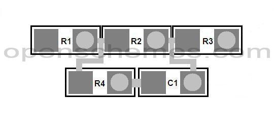
Fig 5 – Pre-Soldering one side of each Padstack
Step 2 – Tacking the components down. For each of the components, use the iron to melt the solder on that first pad.
Then, bring in the component with the tweezers and push it into the solder blob slightly so the solder wicks up onto it’s contact.
You should be able to position the device with the tweezers at this time so it looks nice and is flat against the board.
Remove the iron while still holding the device in place and after a few seconds the solder will cool and you can let go.
Fix any ugliness or misalignment by grabbing again with the tweezers and touching up the solder with the iron.
Don’t let go with the tweezers until the solder is cool, or the device may “tombstone”,
standing up on end due to the thermal contraction of the solder.
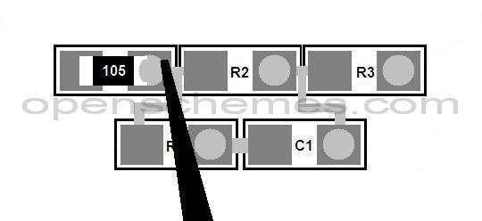
Fig 6 – Tacking the First Side of Each Component
Step 3 – Solder the other side. You can wait until all components are tacked down before doing this, or you can do it one at a time.
The only restriction is that you finish soldering one component before attempting to solder a neighbor with adjoining pads.
In the example here, this means finishing R1 before doing R2. R2 before R3.
This is because heating R2′s left hand may conduct enough heat to melt the right side pad of R1.
Or you may accidentally touch R1 in the process.
If R1 is only held on one side and you melt that side, you may knock it out of alignment or tombstone it.
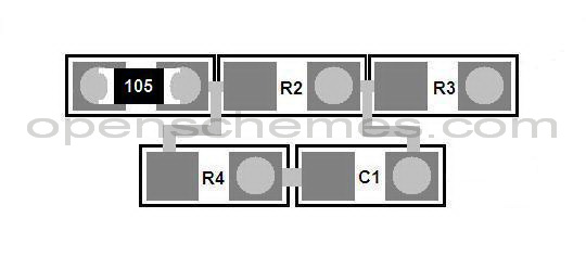
Fig 7 – Completing the Component
Lather, rinse and repeat. You’ll be soldering 160 terminals so you don’t have to put a lot of thought into it,
jut get into a groove and consider it SMT soldering practice. When we look back at our own work,
it seems pretty bad! But the first rule of electical engineering is:
You don’t talk about electrical engineering! Well not to girls at least. They’ll run away.
The 2nd rule of electrical engineering is:
It doesn’t have to be pretty – it has to be conductive.
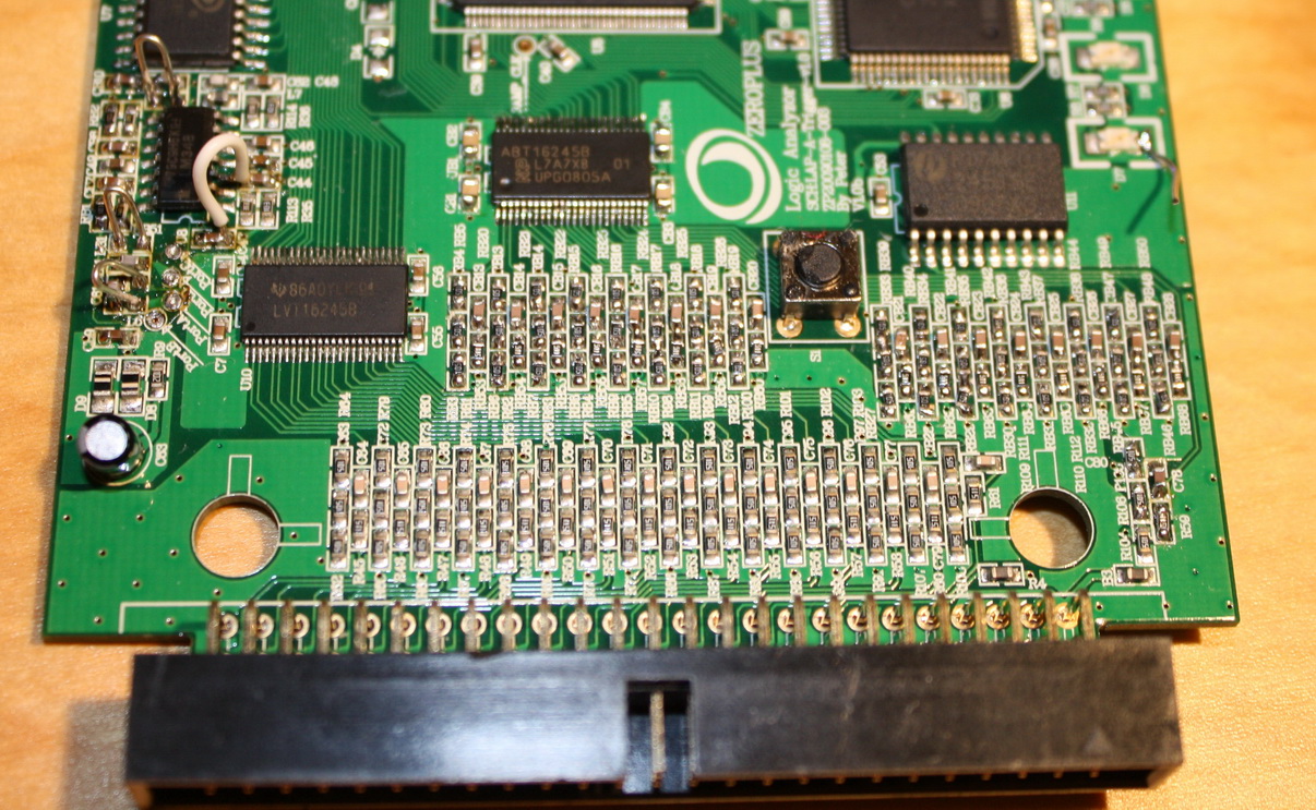
And on that note, we inspect a pic of 16 finished channels on Port C.
You can see the difference between the nice, reflowed, original devices on the left and our shoddy hack on the right.
Also take note of the tinning on the ’245 pads.
That’s the first-pass of the next soldering technique you’ll learn.

Fig 8 – It doesn’t have to be pretty…
Build Details II – 74LVT16245B
Whew! Soldering all those channels must have been monotonous and boring. Maybe you used a toaster-oven reflow. We did not (too much risk to the ASIC we thought) so after installing the new channels we took a night or two off before doing the ’245. Take a break if you need, or keep going while you’re all warmed up – but the 48-TSSOP is not a job to be laughed at.
We’d like to take a moment to discuss the genealogy of the abbreviation “TSSOP”. First, there was the DIP package – Dual Inline Pin. It was a great package and could hold a big old die, but as geometry and die size shrank people wanted something smaller. The SOP (Small Outline Package, sometimes called SO or SOIC) was born. It too was a good package and could be readily soldered by hand. But high lead counts ended up in an unwieldy leadframe (the metal frame the packaged is molded onto). So a new bastard child was born, the Shrink SOIC, or SSOP. Similar proportions to the SOIC but smaller and finer pin pitch. But that device was determined to be too thick for some people (theta-JA and all) and so the THIN Shrink Small Outline Package, or TSSOP was born. It’s thin enough that you can bend it and crack the die if you want, and the lead pitch is pretty damn small. A standard DIP has 100 mil pitch, or 0.1 inch between each pin. The TSSOP has 25 mil pitch, or 4 pins for every DIP pin. GET A FINE POINT SOLDERING IRON TIP.
So here’s how we suggest soldering this beast.
Step 1 - Preparing the pads. Pre-Tin the PCB pads by painting them with flux and wandering over them with a little blob of solder on the iron tip. They should each grab a puddle of solder and look nice and uniformly covered. Now go back and remove almost all the solder using solder wick. Finally, use the iron to wipe any remaining solder out to the outside of the pads. This will create a flat surface that the IC leg can land on, which is essential – if one lumpy pad is preventing the chip from sitting flat, you can get leads that LOOK like they connect but really don’t and the debug is a bitch. The second aspect is that little reservoir of solder at the end of the PCB pad can be wiped back towards the IC to affix the leg once the chip is placed. That tiny pool is all you’ll need. If you try to bring in fresh solder, you’ll probably bridge over 3-4 of the little TSSOP leads. In that case, clean it up with solder wick and retry the wiping.
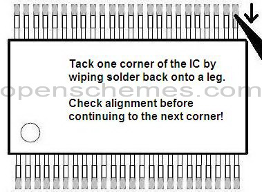
Step 2 – Attaching the chip. Place the TSSOP and align it. One side needs to be PERFECTLY aligned, the other side may wander and tend to drop into the spaces between the PCB pads. That’s OK as we will tack down each side seperately. Apply a little pressure to the top of the chip with your finger, and nudge/lever the body of the chip (don’t apply any pressure to the pins, they will just bend) until all legs on one side are aligned with the pads. Once that is done, use the soldering iron to tack down one corner pin. First, press the pin down with the tip of the iron – this melts the solder under the pin and the solder begins to “wet” the bottom of the pin. Now follow up by wiping from the end of the pad back up over the end of the pin. This should result in a nice sheet of solder covering the end of the pin and up over the bottom of the pin. Some more solder will also wick under the pin due to capillary action. Only do one corner pin at this time!
Step 3 – Tacking the opposing corner. Since only one corner is lightly held, the chip can be moved around a little bit to align the other side. As we said, the other pins usually fall into the gaps between the solder pads on the other side and will need to be adjusted. Stop pressing on the top of the chip for a moment and use your tweezers to adjust the chip so the other side’s pins line up with the
PCB pads. We usually press the sharp tweezer points into the PCB right near the body of the chip and with a little lever action, we can precisely move the chip the fraction of a mm needed to get final alignment. With finger holding the chip in place, tack the opposing corner to freeze the chip placement.
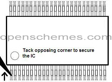
Fig 11 – Tack the other corner once final alignment is completed
Step 4 – Solder the remaining pins, only 46 to go!. You will probably want to generously apply some liquid flux to each row of leads at this point to prevent solder bridges. Use the same technique of pressing each pin down into the pad and then wiping solder back over it. Sometimes, it is helpful to get a tiny speck of solder on the iron and rewipe over each pad-pin connection to insure it is well connected. One speck should last for 4-6 pins at least. You don’t want a drop, you just want the tip wet – no pun intended. But seriously, you can even rewet the iron by touching some other blob of solder like from one of the channels. The tiny layer of residual solder that the iron takes away is plenty for 3-4 pins.
The ’245 also need 4 bypass caps on it’s power supply. These are the pads located above and below the chip. Install 0.1uf or 0.12uF (100nF or 120nF) here, depending on what you have on hand.
Step 5 – Buzz out your board. That’s an old phrase describing the sound a multimeter makes on connectivity mode – beeping when a connection is made. It means to check the connections, of course. It’s a total pain in the ass, but we really suggest you do it to avoid blowing up a chip (or the ASIC) due to a shorted line. In order to touch the TSSOP leads, it’s best to clip onto a sewing needle or something with a very fine point. Stab the needle into the top of each of the TSSOP pins near where it enters the body of the IC. Now use the other lead of the meter to check that pin’s connectivity to the proper channel of the input circuitry. You want to check two things while buzzing out.
- Check that the pin is actually connected to the input circuit (or to the ASIC if you’re checking that side). The meter should beep (of course) when the input circuit and the TSSOP pin are touched. If not, it usually means that the bad pin is not actually soldered down to the PCB pad. That’s why you want to touch the top of the TSSOP pin – to make sure the path is good all the way from the pin, through the PCB trace, to the other circuit.
- Check that the pin is NOT shorted to any adjacent pins. This is easily done by checking the channel adjacent to the pin under test. The pin should NOT be connected to the channel before or after the present one, but it should beep nicely when the present channel is tapped.
An alternate test would be to stab the PCB pad (not the TSSOP pin anymore) and look for a GND->Pin ESD diode. By attaching the red lead of the meter to the PCB GND and stabbing each of the ’245′s PCB pads with the needle, you should see a diode with a value of about 0.5-0.6v pointing from GND to the pad. Again, you stab the pad to make sure the pin in question is well connected to the PCB pad.
You can check the ASIC side by looking at the value of the diode voltage seen. With the ’245′s diode in parallel with the ASIC’s diode the meter should read something like 0.45-0.5v. If you find one pin that is larger (such as 0.6v), then that pin is probably not connected to the ’245 and you’ll need to go back and resolder it.
It’s a good time to mention this if you have not done it already – you will need to cut the shorts between the 16 resistor pads on the back of the PCB now. Actually, you need to do this before you try doing a diode check on the ASIC side. Umm, because they would be shorting all those lines to ground and you would not see ANY diodes in that case. Here’s a pic from after we gouged out those shorts between the resistor pads on the back.
Fig 12 – Cutting the spare channel shorts on the back of the PCB
Fix any shorts by solder-wicking those pins and then resoldering.
Fix any opens by repeating the press, wipe sequence and maybe another speck’s worth of solder.
Buzz out again before continuing.
Build Details III – Trigger Buffers
Fig 3 – Schematic View of the Input Circuit
You’re almost there!
The next circuit that needs to be installed is the op-amp trigger buffers located at the top of the board around the LM348.
Most likely, two channels (A & B) are already installed so you will only have
to solder a few more components in order to complete the hardware.
We’ll start out with the schematic and description of the buffer circuit.
The Zeroplus DV4128B that is located next to the LM348 is a serial DAC used
to provide a variable voltage to the noninverting terminal of each of the 4 op-amps in the ’348.
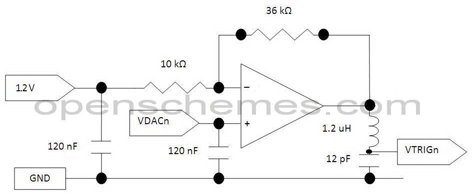
Fig 13 – Schematic of the Trigger Buffer (each channel)
The op-amp will drive it’s output to whatever is needed in order to make the inverting terminal match that DAC voltage.
Since the inverting terminal is connected to a “1.2v reference”,
the difference between that DAC voltage and 1.2v will cause current to flow through the 10k resistor.
And since that current must flow from the op-amp output through the 36k resistor,
the output of the op amp will be VDAC + 3.6 * ( VDAC - 1.2 ).
The 3.6 comes from the ratio between the 10k and the 36k.
In this manner, the output of the op amp can be adjusted both above and below 1.2.
VDAC = 0.0 : 0.0 + 3.6 * ( 0 - 1.2 ) = 3.6 * -1.2 = -4.32
VDAC = 5.0 : 5.0 + 3.6 * ( 5.0 - 1.2 ) = 3.6 * 3.8 = 13.68
This variable output voltage is applied to the top of all the 3x 1MEG resistor dividers in the input circuits for this channel.
In this way, the trip point of the input voltage (trigger threshold) can be varied.
The ’245 always has a fixed input trip point, but the variable buffer voltage
and the input circuit adjusts various input voltage ranges to always match the ’245′s trip point.
The software allows the user to choose TTL, CMOS, ECL, or user-defined levels for the trip point.
It is these selections that determine the DAC and buffer output voltage.
In the interest of completeness, the component layout for all 4 channels of the buffer circuit is shown below.
As was mentioned prior, you will probably only be installing 2 channels,
so some of these components will already be placed – there is no need to move or adjust those devices, obviously.
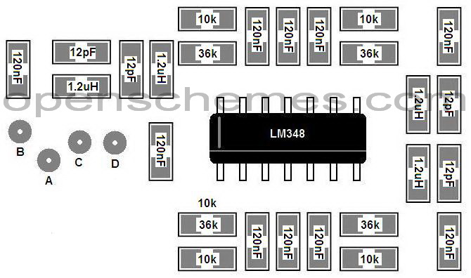
Fig 14 – Component Layout of the Buffer Circuit
In addition to the missing components around the LM348, there are usually two missing capacitors over by the DV4128 DAC.
These are both 120nF capacitors – probably overkill as we are placing parallel VDAC caps near the LM348,
but we went ahead and installed them anyway.
Here’s a pic of our completed buffer circuit. As you may remember,
we lost our 1.2uH inductors or may have left them at the store!
So we installed jumper wires where the 1.2uH inductors would go.
These small wires have SOME inductance, probably 150nH,
but not the right value.
We’ll let you know if skipping these components causes us any problems in the future. Our thinking was:
If digital noise freaks out the LM348, we’ll go get more inductors and install them.
If it kills the ’348, it’s cheap to replace.
So our laziness prevails and in the end we found it works fine.
But our recommendation to you is to install all the proper components unless you’re willing to debug when something goes wrong.

Fig 15 – Final pic of the LAP-C rebuild. A little messy, but works just fine.
You may be wondering about the little white wire jumper on buffer A.
Funny story – the pin next to the noninverting terminal on op-amp A is the negative supply voltage, -12v.
During a probing session, the meter probe slipped off the + terminal and touched between the + terminal and -12v.
This killed channel A of the DAC – blew it clean out and channel A of the DAC just floats dead now.
It’s amazing that the failure mode is a floating open, as we would have guessed
that pulling a 3.3v (probably 0.35um) output to -12v would have latched up the entire DAC chip and turned it into a smoking crater!
The op-amp survived the event unharmed, so we tied his + terminal to the quasi-1.2v reference,
and port A is now hardwired to a 1.2v (TTL) trigger voltage.
That’s fine for us and we are still thanking our lucky stars that ZeroPlus used some kind of structure OTHER
than a CMOS push-pull for their DAC output, or we would have blown the entire DAC.
The moral of the story is:
Be careful when probing a live circuit, folks.
And the second moral is:
If you blow a DAC output, you can always just hardwire the trigger voltage.
Build Details IV – Identity Crisis
We apologize in advance that we’re going to have to punt on this section – the powers that be are giving it a thumbs down. The final part of turning a 16032 into a 32128 is to convince the software that it is talking to an actual 32128. Once the software is convinced that the device has 32 channels and 128k of RAM, it will go fetch 32 channels and 128k of RAM. Now it’s all well and good to solder new resistors onto your board, but “soldering new resistors” into software is somehow seen as distasteful. Meh.
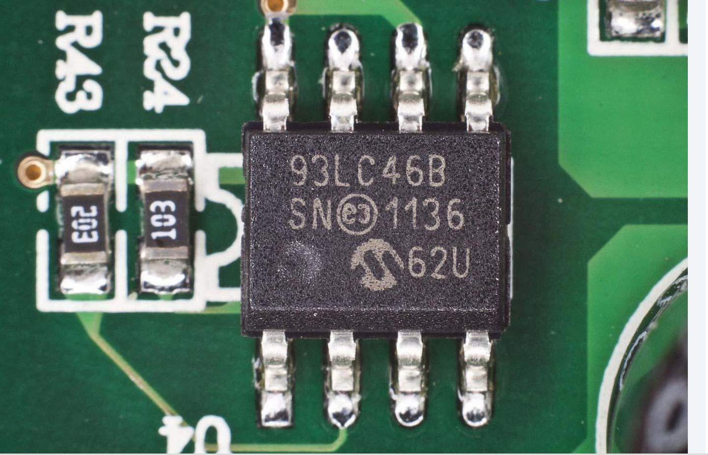
Long story short – you’re on your own here. What we can tell you is that each model has a unique USB PID stored in the 93LC46B serial EEPROM attached to the GL-660 over by the USB jack. The VID/PID is fetched by the software and based on what it finds, the software decides how many channels and how much RAM to fetch when a trigger is detected
We suppose you could try modifying the EEPROM or the software, but again, we don’t know and certainly won’t discuss the details of either. Nor will comments discussing either be allowed. A better route would be to investigate the protocol used to talk to the device so an open-source software replacement could be written! We’re currently trying to drum up interest in this endeavor with some of the folks from other open-source logic analyzer projects, so if you know someone that is a part of those projects or you yourself are part of one, drop us a line and let us know if you’re interested.
Until next time – Happy Hacking!