SN7407
Convert TTL Voltage Levels to MOS Levels
High Sink-Current Capability
Input Clamping Diodes Simplify System Design
Open-Collector Driver for Indicator Lamps and Relays
Inputs Fully Compatible With Most TTL Circuits
These TTL hex buffers/drivers feature high-voltage open-collector outputs
for interfacing with high-level circuits (such as MOS) or
for driving high-current loads (such as lamps or relays) and
also are characterized for use as buffers for driving TTL inputs.
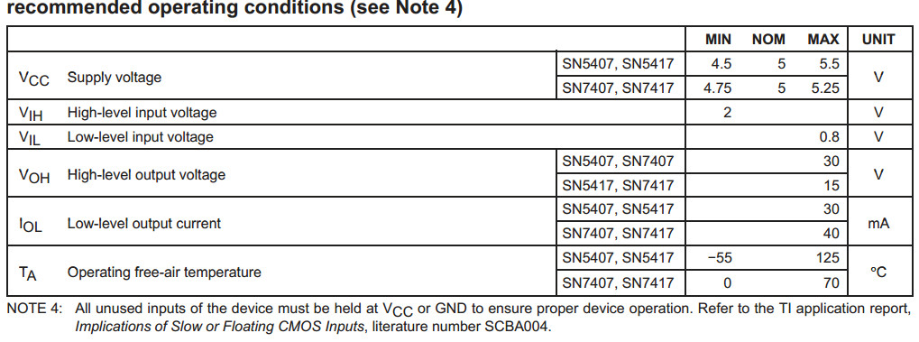
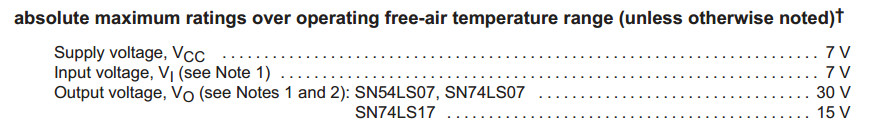
The SN5407 and SN7407 have minimum breakdown voltages of 30 V,
and the SN5417 and SN7417 have minimum breakdown voltages of 15 V.
The maximum sink current is 30 mA for the SN5407
and SN5417 and 40 mA for the SN7407 and SN7417.
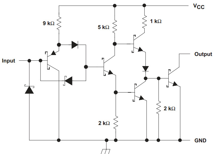
These devices perform the Boolean function Y = A in positive logic.


SN74LS07
These hex buffers/drivers feature high-voltage open-collector outputs
to interface with high-level circuits or for driving high-current loads.
They are also characterized for use as buffers for driving TTL inputs.
The ’LS07 devices have a rated output voltage of 30 V,
and the SN74LS17 has a rated output voltage of 15 V.
The maximum sink current is 30 mA for the SN54LS07
and 40 mA for the SN74LS07 and SN74LS17.
These circuits are compatible with most TTL families.
Inputs are diode-clamped to minimize transmission-line effects,
which simplifies design.
Typical power dissipation is 140 mW and average propagation delay time is 12 ns.
特性
- Convert TTL Voltage Levels to MOS Levels
- High Sink-Current Capability
- Input Clamping Diodes Simplify System Design
- Open-Collector Driver for Indicator Lamps and Relays
The SN54LS07 and SN74LS17 are obsolete and are no longer supplied.

SN54LV07A, SN74LV07A
HEX BUFFERS/DRIVERS
WITH OPEN-DRAIN OUTPUTS
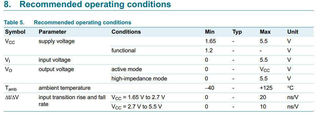
2-V to 5.5-V VCC Operation
Typical VOLP (Output Ground Bounce) <0.8 V at VCC = 3.3 V, TA = 25°C
Typical VOHV (Output VOH Undershoot) >2.3 V at VCC = 3.3 V, TA = 25°C
Outputs Are Disabled During Power Up and Power Down With Inputs Tied to VCC
Support Mixed-Mode Voltage Operation on All Ports
Latch-Up Performance Exceeds 100 mA Per JESD 78, Class II
These hex buffers/drivers are designed for 2-V to 5.5-V VCC operation.
The ’LV07A devices perform the Boolean function Y = A in positive logic.

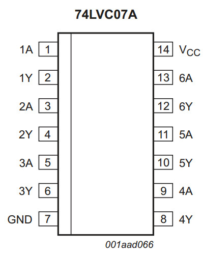
74LVC07A
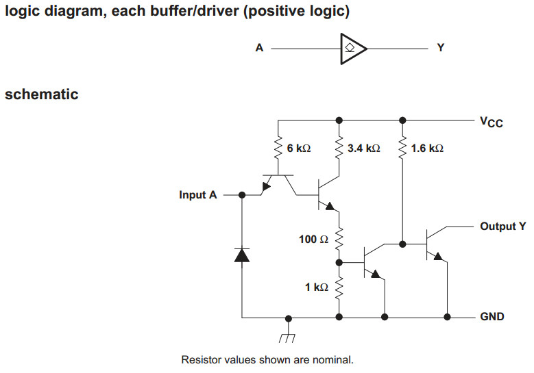
Hex buffer with open-drain outputs
The 74LVC07A provides six non-inverting buffers. The outputs are open-drain and can be
connected to other open-drain outputs to implement active-LOW wired-OR or active-HIGH
wired-AND functions.
Inputs can be driven from either 3.3 V or 5 V devices. This feature allows the use of these
devices as translators in mixed 3.3 V and 5 V applications.
5 V tolerant inputs and outputs (open-drain) for interfacing with 5 V logic
Wide supply voltage range from 1.2 V to 5.5 V
CMOS low power consumption
Direct interface with TTL levels
Inputs accept voltages up to 5 V
Complies with JEDEC standard:
JESD8-7A (1.65 V to 1.95 V)
JESD8-5A (2.3 V to 2.7 V)
JESD8-C/JESD36 (2.7 V to 3.6 V)
ESD protection:
HBM JESD22-A114F exceeds 2000 V
MM JESD22-A115-B exceeds 200 V
CDM JESD22-C101E exceeds 1000 V
Specified from 40 C to +85 C and 40 C to +125 C