转:
NAND Chip Drivers
NAND technology users such as USB pen drives, DOMs, Compact Flash memory, and SD/MMC cards emulate standard storage interfaces such as SCSI or IDE over NAND flash, so you don't need to develop NAND drivers to communicate with them.5 On-board NAND flash chips need special drivers, however, and are the topic of this section.
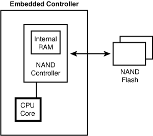
As you learned previously in this chapter, NAND flash chips, unlike their NOR counterparts, are not connected to the CPU via data and address lines. They interface to the CPU through special electronics called a NAND flash controller that is part of many embedded processors. To read data from NAND flash, the CPU issues an appropriate read command to the NAND controller. The controller transfers data from the requested flash location to an internal RAM memory, also part of the controller. The data transfer is done in units of the flash chip's page size (for example, 2KB). In general, the denser the flash chip, the larger is its page size. Note that the page size is different from the flash chip's block size, which is the minimum erasable flash memory unit (for example, 16KB). After the transfer operation completes, the CPU reads the requested NAND contents from the internal RAM. Writes to NAND flash are done similarly, except that the controller transfers data from the internal RAM to flash. The connection diagram of NAND flash memory on an embedded device is shown in Figure 17.3.
Because of this unconventional mode of addressing, you need special drivers to work with NAND storage. MTD provides such drivers to manage NAND-resident data. If you are using a supported chip, you have to enable only the appropriate low-level MTD NAND driver. If you are writing a NAND flash driver, however, you need to explore two datasheets: the NAND flash controller and the NAND flash chip.
NAND flash chips do not support automatic configuration using protocols such as CFI. You have to manually inform MTD about the properties of your NAND chip by adding an entry to thenand_flash_ids[] table defined in drivers/mtd/nand/nand_ids.c. Each entry in the table consists of an identifier name, the device ID, page size, erase block size, chip size, and options such as the bus width.
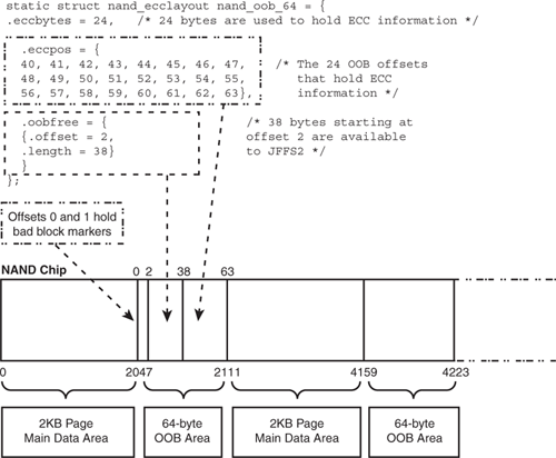
There is another characteristic that goes hand in hand with NAND memory. NAND flash chips, unlike NOR chips, are not faultless. It's normal to have some problem bits and bad blocks scattered across NAND flash regions. To handle this, NAND devices associate a spare area with each flash page (for example, 64 bytes of spare area for each 2KB data page). The spare area contains out-of-band (OOB) information to help perform bad block management and error correction. The OOB area includes error correcting codes (ECCs) to implement error correction and detection. ECC algorithms correct single-bit errors and detect multibit errors. The nand_ecclayout structure defined ininclude/mtd/mtd-abi.h specifies the layout of the OOB spare area:
struct nand_ecclayout {
  uint 32_t eccbytes;
  uint32_t  eccpos[64];
  uint32_t  oobavail;
  struct    nand_oobfree oobfree[MTD_MAX_OOBFREE_ENTRIES];
};
In this structure, eccbytes holds the number of OOB bytes that store ECC data, and eccpos is an array of offsets into the OOB area that contains the ECC data. oobfree records the unused bytes in the OOB area available to flash filesystems for storing flags such as clean markers that signal successful completion of erase operations.
Individual NAND drivers initialize their nand_ecclayout according to the chip's properties. Figure 17.4illustrates the layout of a NAND flash chip having a page size of 2KB. The OOB semantics used by the figure is the default for 2KB page-sized chips as defined in the generic NAND driver,drivers/mtd/nand/nand_base.c.
Often, the NAND controller performs error correction and detection in hardware by operating on the ECC fields in the OOB area. If your NAND controller does not support error management, however, you will need to get MTD to do that for you in software. The MTD nand_ecc driver (drivers/mtd/nand/nand_ecc.c) implements software ECC.
Figure 17.4 also shows OOB memory bytes that contain bad block markers. These markers are used to flag faulty flash blocks and are usually present in the OOB region belonging to the first page of each block. The position of the marker inside the OOB area depends on the properties of the chip. Bad block markers are either set at the factory during manufacture, or by software when it detects wear in a block. MTD implements bad block management in drivers/mtd/nand/nand_bbt.c.
The mtd_partition structure used in Listing 17.1 for the NOR flash in Figure 17.2 works for NAND memory, too. After you MTD-enable your NAND flash, you can access the constituent partitions using standard device nodes such as /dev/mtd/X and /dev/mtdblock/X. If you have a mix of NOR and NAND memories on your hardware, X can be either a NOR or a NAND partition. If you have a total of more than 32 flash partitions, accordingly change the value of MAX_MTD_DEVICES ininclude/linux/mtd/mtd.h.
To effectively make use of NAND storage, you need to use a filesystem tuned for NAND access, such as JFFS2 or YAFFS2, in tandem with the low-level NAND driver. We discuss these filesystems in the next section.