Timing Analysis in the Design Flow
设计流程中的时序分析
在设计流程的不同阶段,时序分析有不同的目的。在DC中,时序驱动着用于综合的库单元的选择以及数据路径中的组合逻辑之间的寄存器的分配。在ICC中,时序驱动着单元的布局和互连线的布局,以实现关键路径上的延迟最小化。在PT中,详细的签核(sign-off)时序分析是该工具的主要目的。这些工具共同使用者同样的基础延迟计算方法。时序分析的结果在通常情况下是一致的,但不总是完全相同的。因为PT是一个签核(sign-off)时序分析工具,它会进行更加全面透彻的分析去验证正确的时序,而DC与ICC工作时,以满足驱动综合,物理实现,以及优化的足够精度为目标即可。
Timing analysis serves different purposes in different phases of the design flow. In Design Compiler, timing drives the selection of library cells used for synthesis and the allocation of registers between combinational logic in data paths. In IC Compiler, timing drives the placement of cells and the routing of interconnections to minimize delays in the critical paths.In PrimeTime, exhaustive sign-off timing analysis is the main purpose of the tool.These tools all share the same basic delay calculation methods. The timing results are generally consistent between the tools but not always identical. Because PrimeTime is a sign-off analysis tool, it performs a more comprehensive and exhaustive analysis to verify correct timing, whereas Design Compiler and IC Compiler perform timing analysis with sufficient accuracy to drive synthesis, physical implementation, and optimization.

synopsys 设计约束命令
Synopsys Design Constraint Commands
DC,ICC和PT有许多共同的时间分析功能。这些工具允许您使用相同的命令来指定时序约束和生成时序报告。这些命令称为Synopsys设计约束(SDC)。这些命令具有相同的语法,并在所有支持的工具中产生相同的效果。这意味着您可以使用相同的SDC脚本在DC、ICC、PT和其他工具中约束设计。SDC命令可以指定设计规则约束、功率约束以及时间约束。
Design Compiler, IC Compiler, and PrimeTime share many common timing analysis features. The tools allow you to use the same commands to specify timing constraints and generate timing reports. These commands are known as the Synopsys Design Constraints (SDC). These commands have the same syntax and produce the same effects across all the supported tools. That means you can use the same SDC script to constrain a design in Design Compiler, IC Compiler, PrimeTime, and other tools. The SDC commands can specify design rule constraints and power constraints as well as timing constraints.
在每个工具中,可以用write_sdc命令写出一个脚本,该脚本包含一组SDC命令,这些命令在当前设计上设定约束。在另一种工具中,可以使用read_sdc命令读取文件并应用相同的约束。read_sdc命令的工作方式与source命令非常相似,但是read_sdccommand也会检查脚本命令是否符合SDC规则。SDC脚本文件可以用于在Synopsys工具和某些外部工具之间传输约束。
In each tool, the write_sdc command writes out a script containing a set of SDC commands that specify the current constraints set on the design. In a different tool, you can use the read_sdc command to read in the file and apply the same constraints. The read_sdc command works very much like the source command, but the read_sdccommand also checks the script commands for SDC compliance. SDC script files can be used to transfer constraints between Synopsys tools and also certain external tools.
一些Synopsys工具以扩展命令或命令选项的形式扩展了SDC所支持的约束功能。write_sdc命令只写出与sdc兼容的命令,这些命令可以在任意SDC格式兼容的工具上执行。而write_script命令会写出更大范围的用于设置设计属性的指令。
Some Synopsys tools have extended constraint capabilities beyond what is supported by SDC in the form of additional commands or command options. The write_sdc command writes out only the SDC-compatible commands, which can be executed in any SDC-compatible tool. The write_script command writes out a wider range of commands that set the design attributes.
为了帮助追踪已设置的约束,一些SDC命令可允许将注释字符串与约束关联。要添加注释,需使用-commentoption 选项注释字符串。例如,命令行> create_clock -name"CLK"-周期 0.33 -注释"Main clock"。注释在整个设计、分析和实现流程中都得到保留。每次使用write_sdc或write_script命令时,该工具使用相同的注释字符串使用-comment选项写出SDC命令。
To help keep track of constraints that have been set, some SDC commands optionally allow a comment string to be associated with the constraint. To add a comment, use the -commentoption along with a comment string. For example,
prompt> create_clock -name "CLK" -period 0.33 -comment "Main clock"
The comment is maintained throughout the design, analysis, and implementation flow. Each time you use the write_sdc or write_script command, the tool writes out the SDC command with the -comment option using the same comment string.
要从设计中删除所有的synopsys设计约束,可以使用remove_sdc命令。表1-1列出了用于指定时间约束和与时间相关的设计特性的SDC命令。有关SDC命令的更多信息,请参见使用Synopsys设计约束格式应用手册,它可以在SolvNet的Design Compiler、IC Compiler和PrimeTime文档集中找到。要访问SolvNet,请访问SolvNet的网页,网址如下: https://solvnet.synopsys.com
To remove all Synopsys Design Constraints from the design, use the remove_sdc command.Table 1-1 lists the SDC commands used for specifying timing constraints and timing-related design characteristics. For more information about SDC commands, see the Using the Synopsys Design Constraints Format Application Note, which is available on SolvNet in the documentation sets for Design Compiler, IC Compiler, and PrimeTime. To access SolvNet, go to the SolvNet Web page at the following address: https://solvnet.synopsys.com
表1-1 SDC时序命令
Table 1-1 SDC Timing Commands
|
Command/命令 |
Usage/用法 |
用法中文说明 |
|
create_clock |
Specifies the clocks used in the design and their characteristics: |
指定在设计中使用的时钟及其特性:名称、周期、波形和在设计中的位置。时间分析器需要此信息来确定每个路径端点所需的数据到达时间。 |
|
prompt> create_clock "PHI1" -period 10 -waveform {5.0 9.5} |
||
|
group_path |
Groups a set of paths or endpoints for timing analysis and cost |
对一组路径或端点进行分组,以便进行时序分析和(时间)花销函数计算。包含在一个组内路径的分析和优化是独立于其他组的。默认情况下,每个时钟有一个路径组。 |
|
prompt> group_path -name "group1" -weight 2.0 -to {CLK1A CLK1B} |
||
|
set_clock_gating_check |
Creates one or more clock-gating checks in the design. A |
在设计中创建一个或多个时钟控制检查。时钟门控检查是对时钟门控单元的控制输入执行的建立或保持时间检查。它检测发生了时钟边缘截断或假时钟脉冲。 |
|
prompt> set_clock_gating_check -setup 0.75 -hold 0.5 |
||
|
set_clock_groups |
Specifies groups of clocks that are mutually exclusive or |
指定互相排斥或异步的时钟组。这可以防止分析从一个时钟组开始到另一个时钟组结束的时序路径。 |
|
set_clock_groups -asynchronous -name g1 -group CLK1 -group CLK2 |
||
|
set_clock_latency |
Specifies explicitly the source latency or network latency of a clock. This command is typically used before layout, when propagated clocking cannot be used. Source latency is the time the clock signal takes to be propagated from its ideal waveform origin point to the clock definition point in the design. Network latency is the time the clock signal takes to be propagated from the clock definition point in the design to the clock pin of the sequential device. The timing analyzer uses this information to determine clock arrival times in the absence of propagated clocking. |
显式指定时钟的源延迟或网络延迟。此命令通常在布局之前使用,此时经过传播后的时钟信息还无法获得。源延迟是时钟信号从理想波形点传播到设计中的时钟定义点所需的时间。网络延迟是时钟信号从设计中的时钟定义点传播到时序设备的时钟pin的时间。在没有传播时钟的情况下,定时分析器使用此信息来确定时钟到达时间。 |
|
prompt> set_clock_latency 1.2 -rise [get_clocks CLK1] prompt> set_clock_latency 0.9 -fall [get_clocks CLK1] |
||
|
set_clock_sense |
Specifies the unateness of a clock signal, either positive or negative,that is propagated past a nonunate point in the clock network. A nonunate point is a place where the sense of the clock signal cannot be determined, such as the output of an exclusive OR gate with the clock signal as one input and an unknown side-input value as the other input. |
指定时钟信号(正的或负的)的不适当性,该时钟信号在时钟网络中传播过一个nonunate点。nonunate点是一个时钟信号的感觉不能被确定的地方,例如一个时钟信号作为一个输入和一个未知的边输入值作为另一个输入的排他性或门的输出。 |
|
set_clock_sense -positive -clocks [get_clocks CLK1] XOR/Z |
||
|
set_clock_transition |
Specifies explicitly the rising or falling transition times of a clock. This command is typically used before layout, when propagated clocking cannot be used. The transition time applies to rising or falling transitions at the clock pins of sequential devices clocked by the specified clock. The timing analyzer uses this information to |
显式指定时钟的上升或下降转换时间。此命令通常在布局之前使用,此时经过传播后的时钟信息还无法获得。该过渡时间适用于由指定时钟计时的顺序设备的时钟插脚处的上升或下降过渡。在没有传播时钟的情况下,定时分析器使用此信息来确定时钟转换时间 |
|
set_clock_transition 0.75 CLK |
||
|
set_clock_uncertainty |
Specifies the uncertainty or skew characteristics of a single clock or |
指定单个时钟或两个不同时钟之间的不确定性或偏移特性。对于一个时钟,简单的不确定性是连续的边缘之间的最大差异的变化远离名义到达时间。对于两个时钟,时钟间不确定度是时钟边缘出现时相对于标称到达时间的变化的最大差异或歪斜。时序分析仪使用此信息来确定每次定时检查的最坏时钟到达时间。 |
|
prompt> set_clock_uncertainty -setup 0.65 [get_clocks CLK] prompt> set_clock_uncertainty -hold 0.45 [get_clocks CLK] |
||
|
set_data_check |
Creates a custom data-to-data check, also known as a nonsequential constraint, using specified setup and hold time values between the specified data signals. You specify the "from" object or related pin, the "to" object or constrained pin, and the setup or hold value for the check |
使用指定的数据信号之间的建立与保持时间值,创建自定义数据至数据路径的检查,也称为非顺序约束。您可以指定"from"对象或相关pin、"to"对象或约束pin以及用于检查的建立时间或h保持时间值 |
|
prompt> set_data_check -rise_from and1/B -to and1/A 0.4 |
||
|
set_disable_timing |
Disables timing checks and timing optimization for specified cells, |
禁用指定单元格、引脚或端口的定时检查和定时优化。这个命令完全从时间分析中删除受影响的对象,这与set_false_path命令不同,set_false_path命令只从路径中删除时序约束,而不删除延迟计算。如果通过一个引脚的所有路径都为假,set_disable_timing比set_false_path更有效。 |
|
set_disable_timing {U2 U3} |
||
|
set_driving_cell |
Specifies the name of a library cell that drives one or more input ports of the design. This information allows the timing analyzer to |
指定驱动设计的一个或多个输入端口的库单元的名称。这些信息允许定时分析仪准确地确定由驱动程序、负载和网络的线特性引起的延迟。 |
|
prompt> set_driving_cell -lib_cell INV -pin Z -library tech_lib [all_inputs] |
||
|
set_fanout_load |
Specifies the number of external loads in the fanout of one or more |
指定设计的一个或多个输出端口扇出中的外部负载数量。该工具使用这些信息来执行最大扇出设计规则,而不是执行时间分析。 |
|
prompt> set_fanout_load 2 all_outputs() |
||
|
set_ideal_latency |
Specifies explicitly the ideal clock latency in the transitive fanout of |
显式指定指定端口或引脚的传递扇形中的理想时钟延迟。理想时钟延时是一个时钟信号从它的理想波形原点传播到一个理想网络中顺序设备的时钟针所需要的时间。默认的理想延迟为零。在没有传播时钟的情况下,定时分析工具使用理想延迟来确定时钟到达时间。 |
|
prompt> set_ideal_latency 1.2 -rise {A B C} prompt> set_ideal_latency 0.9 -fall {A B C} |
||
|
set_ideal_network |
Invokes ideal clocking behavior in the transitive fanout of specified |
在指定端口、引脚或网络的传递扇形中调用理想的时钟行为,导致在指定的整个网络中显式指定的延迟和转换时间(默认为零)。理想时钟在布局之前使用,当传播时钟不能使用时。 |
|
prompt> set_ideal_network {port1 port2} |
||
|
set_ideal_transition |
Specifies explicitly the rising or falling transition times of signals in the transitive fanout of specified ports or pins. The default ideal transition time is zero. The timing analysis tool uses the ideal transition time in the absence of propagated clocking. |
显式指定在指定端口或引脚的传递扇形中信号的上升或下降过渡时间。默认的理想过渡时间为零。定时分析工具在没有传播时钟的情况下使用理想的转换时间。 |
|
prompt> set_ideal_transition 1.2 -rise {A B C} |
||
|
set_input_delay |
Specifies the amount of delay from a launch clock edge outside of the design to the arrival of data at an input of the design. This information is necessary to check the timing of signals entering the design inputs. |
指定从设计之外的发射时钟边缘到数据到达设计的输入端的延迟量。这些信息对于检查进入设计输入信号的时间是必要的。 |
|
prompt> set_input_delay 2.3 {IN1 IN2} prompt> set_input_delay 1.2 -clock [get_clocks CLK1] [all_inputs] |
||
|
set_input_transition |
Specifies explicitly the rise or fall transition times on input ports of the design for propagated (not ideal) clocking. The timing analyzer uses this information to determine the delays and transition times of signals in the transitive fanout of the input. |
为传播(不是理想的)时钟显式指定设计的输入端口上的上升或下降过渡时间。定时分析仪使用这些信息来确定输入信号的传递扇形的延迟和过渡时间。 |
|
prompt> set_input_transition 7.0 {A B C} |
||
|
set_load |
Specifies explicitly the capacitive load on one or more input ports, |
显式指定一个或多个输入端口、输出端口或网络上的电容负载。定时分析仪使用这些信息来确定负载对信号通过端口或网络的延迟和转换时间的影响。 |
|
prompt> set_load -subtract_pin_load 3 U1/U2/NET3 prompt> set_load -wire_load 5 the_answer |
||
|
set_operating_conditions |
Specifies the operating conditions under which the design is |
说明在设计分析和优化的操作条件。库定义了操作条件,每个条件由一组工艺、温度和电压值组成。库中的每个单元对于每个操作条件都有一组不同的单元定时特性。该命令根据名称选择这些定义的操作条件中的一个或多个,并调用最佳情况/最差情况分析或片上变化分析。 |
|
prompt> set_operating_conditions -min BCIND -max WCIND -library other_lib_core |
||
|
set_output_delay |
Specifies the amount of delay from the departure of data at an output of the design to the capture clock edge outside the design. This information is necessary to check the timing of signals leaving the design outputs. |
指定从设计输出的数据离开到设计之外的捕获时钟边缘的延迟量。这些信息对于检查离开设计输出信号的时间是必要的。 |
|
prompt> set_output_delay 1.7 -clock [get_clocks CLK1] [all_outputs] |
||
|
set_port_fanout_number |
Specifies the number of external loads in the fanout of one or more |
指定设计的一个或多个输出端口扇出中的外部负载数量。这允许定时分析仪估计连接到输出的外部设备的总线负载。 |
|
prompt> set_port_fanout_number 5 [get_ports O1] |
||
|
set_propagated_clock |
Causes network latency to be determined by propagating delays |
使网络延迟由传播延迟通过时钟网络为指定的时钟或为过渡离开指定的端口或针。当详细的网RC信息可用时,传播的时钟可以在布局之后使用。 |
|
prompt> set_propagated_clock [all_clocks] |
||
|
set_resistance |
Specifies explicitly the resistance of one or more nets. The timing |
显式指定一个或多个网的电阻。时序分析器使用这些信息来确定在延迟和过渡电阻的影响时间的信号通过。 |
|
prompt> set_resistance 200 {a b} |
||
|
set_timing_derate |
Applies derating or adjustment factors to specified delays of timing |
对时间检查的指定延迟应用减损或调整因素。降额可以用来模拟过程、电压和温度变化的最坏情况的影响。 |
|
prompt> set_timing_derate -max -early -net_delay 0.9 |
||
|
set_wire_load_model |
Specifies the types of wire load models used for estimating wire |
指定在执行布线之前用于估计线阻和电容的线负载模型的类型。用于设计编译器和黄金时间;不用于使用拓扑模式的DC或ICC环境中。 |
|
prompt> set_wire_load_model -name "10x10" -library my_lib.db |
||

Library Timing Data
库时序数据
为了进行时序分析,该工具需要得到设计中使用的逻辑单元的时序特性的信息,如组合逻辑块的输入输出延迟;时序模块的时钟到输出延迟、建立时间和保持时间;和单元输出信号的转换时间。单元的时序特性包含在每个单元的库描述中。时序分析工具可以以以下形式读取库数据:
•使用read_lib命令的Liberty (.lib)格式
•使用read_db或read_file命令格式化Synopsys数据库(.db)
To perform timing analysis, the tool needs information about the timing characteristics of the logic cells used in the design, such as the input-to-output delays of combinational logic blocks; clock-to-output delays, setup times, and hold times of sequential blocks; and transition times of cell output signals. The cell timing characteristics are contained in the library description of each cell. Timing analysis tools can read the library data in the following forms:
• Liberty (.lib) format using the read_lib command
• Synopsys database (.db) format using the read_db or read_file command
单元时序特性通常使用一个特性描述工具(如Liberty NCX)与电路模拟器(如HSPICE)相结合来确定。Liberty NCX以Liberty (.lib)格式输出单元时间数据,这是一种人们可以读取的文本格式。一些时序分析工具可以使用read_lib命令直接读取.lib文件。库编译器(LB)通常将Liberty (.lib)格式的库编译为Synopsys数据库(.db)格式。db文件是一种二进制格式,比.lib格式更紧凑,读取速度更快。时序分析工具可以通过read_db命令直接读取.db库,也可以通过link_library变量设置隐式读取。每个单元时序参数,如输入到输出的延迟或输出转换时间,是输入摆率和输出负载的函数。因此,延迟信息被组织在与输入摆率和输出负载的不同组合相对应的值的表中。如果该表可用,您可以在.lib库文件中查看时序参数表。您还可以使用report_lib -timing命令在分析工具中查看计时数据。例如:
The cell timing characteristics are typically determined by a characterization tool such as Liberty NCX in combination with a circuit simulator such as HSPICE. Liberty NCX writes out the cell timing data in Liberty (.lib) format, a text format that a person can read. Some timing analysis tools can read .lib files directly with the read_lib command. Libraries in Liberty (.lib) format are typically compiled into Synopsys database (.db) format by Library Compiler. The .db file is a binary format that is more compact and faster to read than the .lib format. A timing analysis tool can read in a .db library directly with the read_db command or implicitly via the link_library variable setting.Each cell timing parameter, such as input-to-output delay or output transition time, is a function of the input slew and output load. Accordingly, the delay information is organized in a table of values corresponding to different combinations of input slew and output load. You can view the timing parameter tables in the .lib library file, if available. You can also view the timing data in the analysis tool by using the report_lib -timing command. For example,
prompt> report_lib -timing cb13fs120_max nd02d1
...
Lookup Table Template:
Template_name
--------------------------------------------------------------------
del_1_5_7_w
VARIABLE_1: input_net_transition
VARIABLE_2: total_output_net_capacitance
INDEX_1: 0.0150 0.2500 0.6500 1.4000 3.0000
INDEX_2: 0.0000 0.0070 0.0140 0.0385 0.0805 0.1505 0.3500
...
DELAY: A2, ZN, prop, neg_unate, '', ( , ), ( , ), ( , );
cell_rise ( del_1_5_7_w ) :
VALUES : 0.0270 0.0480 0.0690 0.1400 0.2620 0.4650
1.0420 0.0680 0.0990 0.1230 0.1950 0.3160
0.5190 1.0970 0.1010 0.1510 0.1890 0.2870
0.4110 0.6140 1.1910 0.1380 0.2080 0.2630
0.4060 0.5790 0.7920 1.3670 0.1880 0.2860
0.3620 0.5660 0.8170 1.1270 1.7480
该表列出了从输入A2到输出ZN的上升信号的延迟值,以及从索引表中获取的输入过渡时间和输出电容负载的每个可能组合。延迟计算器使用插值或外推来获得索引表之间或外部的输入转换时间和电容负载的延迟值。类似的表将输出转换时间指定为输入转换和输出加载的函数。为一个单元计算的输出转换时间将成为计时路径中下一个单元的输入转换时间。对于设计中特定单元实例或网络的延迟计算的详细描述,可以使用report_delay_calculation命令。例如,
The table lists the delay values from the input A2 to the output ZN for a rising signal, for each possible combination of an input transition time and an output capacitive load taken from the index tables. The delay calculator uses interpolation or extrapolation to get delay values for input transition times and capacitive loads between or outside of the index tables. Similar tables specify the output transition times as a function of input transition and output load. The output transition time calculated for a cell becomes the input transition time for the next cell in the timing path.For a detailed description of the delay calculation for a particular cell instance or net in the design, you can use the report_delay_calculation command. For example,
prompt> report_delay_calculation -from I_RISC_CORE/I_ALU/U27/A2
-to I_RISC_CORE/I_ALU/U27/ZN
...
Rise Delay
cell delay = 0.0583731
Table is indexed by
(X) input_pin_transition = 0.103374
(Y) output_net_total_cap = 0.00451049
Relevant portion of lookup table:
(X) 0.0150 (X) 0.2500
(Y) 0.0000 (Z) 0.0270 (Z) 0.0680
(Y) 0.0070 (Z) 0.0480 (Z) 0.0990
Z = A + B*X + C*Y + D*X*Y
A = 0.0244 B = 0.1745
C = 2.9088 D = 6.0790
Z = 0.0583731
scaling result for operating conditions
multiplying by 1 gives 0.0583731
...
单元延迟随运行条件的不同而不同,因此库对于不同的运行条件角可能有不同的延迟值。条件角是电压、温度和工艺值(PVT)的特殊组合。一些库是为缩放而设计的,以便分析工具可以通过在定义的操作条件及其对应的延迟值之间进行插值来获得中间操作条件下的准确延迟值。
Cell delays vary with operating conditions, so the libraries may have different delay values for different operating condition corners. A corner is a particular combination of voltage, temperature, and process values(PVT). Some libraries are designed for scaling so that the analysis tool can obtain accurate delay values at intermediate operating conditions by using interpolation between the defined operating conditions and their corresponding delay values.

Design Compiler
DC是一个用于将RTL(寄存器传输级)描述的设计转换为门级网表的工具。DC所执行的综合过程主要包括下列步骤:
•读入Verilog或VHDL格式的RTL描述。
•以Synopsys设计约束(SDC)格式读取时序,面积和功率约束。
•使用通用布尔逻辑门生成设计逻辑,优化逻辑,然后使用目标库中指定工艺的门将设计映射到网表中。
•以.ddc格式写出已编译的门级网表。
Design Compiler is a synthesis tool that converts a design description at the Register Transfer Level (RTL) to a gate-level netlist. The synthesis process performed by Design Compiler typically consists of the following major steps:
• Read in the RTL description in Verilog or VHDL format.
• Read in the timing, area, and power constraints in Synopsys Design Constraints (SDC) format.
• Generate the design logic using generic Boolean gates, optimize the logic, and map the design into a netlist using the technology-specific gates of the target library.
• Write out the compiled gate-level netlist in .ddc format.
尽管面积和功率限制很重要,但只有时序限制必须绝对满足才能使电路工作。 时序驱动逻辑实现和从库中选择门,以确保时序路径延迟不超过适用的时钟周期。 例如,在发现设置延迟过长的情况下,Design Compiler可能会使用具有更大驱动强度的大型设备来减少净延迟,但会占用更多的面积。
Although the area and power constraints are important, only the timing constraints must be absolutely satisfied for the circuit to operate. Timing drives the logic implementation and selection of gates from the library to ensure that timing path delays do not exceed the applicable clock periods. For example, where a setup delay is found to be too long, Design Compiler might use larger devices with more drive strength to reduce net delays, at the expense of more area.
在将时序约束应用于设计之后,应使用check_timing命令检查时序约束和设置问题。 综合完成后,您可以报告最坏情况的路径,并使用report_constraintand report_timing命令进行详细分析。
After you apply the timing constraints to the design, you should check for timing constraint and setup problems with the check_timing command. After synthesis is completed, you can report the worst-case paths and analyze them in detail with the report_constraintand report_timing commands.

理想时钟
Ideal Clocking
在布局之前的逻辑综合阶段,执行时钟树综合是不切实际的,因为导线长度未知,并且时钟偏斜对寄生互连差异非常敏感。 默认情况下,Design Compiler使用理想的时钟,这意味着所有时钟信号的等待时间为零,不确定性为零,过渡时间为零。 延迟是从时钟源到时钟寄存器引脚的延迟,对于零时钟,理想时钟基于零电阻和时钟网络电容的假设为零。 时钟网络中的所有网络和单元都会自动标记为dont_touch。 理想的网络在合成过程中没有得到优化或缓冲。 理想的时钟非常乐观。 为了获得更准确的时序结果,您可以为时钟信号指定非零延迟,不确定性和转换时间,以代表完整时钟网络预期的近似时序值。 例如,
At the logic synthesis stage before layout, performing clock tree synthesis is not practical because the wire lengths are unknown and the clock skew is highly sensitive to parasitic interconnect differences. By default, Design Compiler uses ideal clocking, which means zero latency, zero uncertainty, and zero transition time for all clock signals. Latency is the delay from the clock source to the clock register pins, which is zero for ideal clocking, based on the assumption of zero resistance and capacitance of the clock network. All nets and cells in the
clock network are automatically marked as dont_touch. Ideal networks are not optimized or buffered during synthesis. Ideal clocking is highly optimistic. To get more accurate timing results, you can specify nonzero latency, uncertainty, and transition times for clock signals to represent the approximate timing values expected for the completed clock network. For example,
dc_shell> set_clock_latency 1.2 -rise [get_clocks CLK1]
dc_shell> set_clock_latency 0.9 -fall [get_clocks CLK1]
dc_shell> set_clock_uncertainty -setup 0.65 [get_clocks CLK1]
dc_shell> set_clock_uncertainty -hold 0.45 [get_clocks CLK1]
dc_shell> set_clock_transition 0.34 -rise [get_clocks CLK1]
dc_shell> set_clock_transition 0.30 -fall [get_clocks CLK1]
通过这样的设置,时钟网络仍然被认为是理想的,但是在整个时钟网络中指定的延迟,不确定性和偏斜值而不是零。 除时钟以外的高扇出网络(例如复位或启用信号)可能还需要在布局阶段而不是在Design Compiler中合成的缓冲树。 对于这些网络,可以在布局工具中预期高扇出网络综合的情况下,指定理想的网络行为以及非零延迟和过渡时间以进行综合。 例如,
dc_shell> set_ideal_network [get_ports Reset]
dc_shell> set_ideal_latency 1.40 [get_ports Reset]
dc_shell> set_ideal_transition 0.30 [get_ports Reset]
线负载模型与拓扑技术
Wire Load Models and Topographical Technology
为了执行准确的时序分析,必须知道信元延迟和净延迟。但是,在预布局逻辑综合阶段,由于导线长度未知,因此无法确定确切的净延迟。您可以使用两种方法来估计Design Compiler中的RC导线特性:导线负载模型和地形技术。线负载模型会根据网络的扇出,为每个网络获得一个寄生电阻值和一个电容值。扇出较大的网络被假定具有更多的导线,因此具有更多的电阻和电容。线负载模型在技术库中提供。这些模型基于从相似设计中提取的数据,这些数据采用相同的工艺技术制造,尺寸相似。一个库通常具有多个线负载模型,以用于不同的设计尺寸。随着设计尺寸的增加,标准单元可以在该设计中物理上分开放置,这意味着导线长度通常会更长。一些库供应商可能会在其模型中使用名称来表示不同的设计尺寸,例如" 300kGates"," 600kGates"等等。根据尺寸为设计选择合适的线负载模型很重要。例如,
To perform accurate timing analysis, both cell delays and net delays must be known. However, at the prelayout logic synthesis stage, the exact net delays cannot be determined because the wire lengths are unknown. There are two methods you can use to estimate the RC wire characteristics in Design Compiler: wire load models and topographical technology. A wire load model obtains one parasitic resistance value and one capacitance value for each net, based on the net's fanout. A net having a larger fanout is assumed to have more wires and therefore more resistance and capacitance. Wire load models are supplied in the technology library. The models are based on data extracted from similar designs for similar size, fabricated with the same process technology. A library typically has several wire load models to be used for different design sizes. As the size of a design increases, standard cells can be placed physically farther apart within that design, which means that wire lengths are typically longer. Some library vendors may use names for their models to represent different design sizes, such as "300kGates,"600kGates," and so on. It is important to select the appropriate wire load model for the design according to size. For example,
dc_shell> set_wire_load_model -name 1.6MGates
指定的模型适用于当前设计级别及以下的所有网络。 当设计是分层的并且模块被分组到芯片的物理区域时,较小的单个线负载模型可以更好地表示每个较低级别子设计中的实际RC值。 例如,
The specified model applies to all nets at the current design level and below. When the design is hierarchical and the blocks are grouped into physical areas of the chip, then smaller individual wire load models can better represent the actual RC values within each lower-level subdesign. For example,
dc_shell> set_wire_load_model -name 1.6MGates
dc_shell> set_wire_load_mode enclosed
dc_shell> set_wire_load_model -name 800KGates [get_designs SUB1]
dc_shell> set_wire_load_model -name 200KGates [get_designs B1]
dc_shell> set_wire_load_model -name 100KGates [get_designs B2]
将线负载模式设置为"封闭"意味着,使用在完全包围该网的最小子设计上设置的线负载模型来计算每个网的线电容。 一些库支持基于设计区域的自动线负载选择。可以通过auto_wire_load_selection变量控制此功能的使用。 线负载模型基于统计平均值,并不特定于特定设计。 在超深亚微米设计中,由于导线寄生物对路径延迟的影响增加,导线负载模型可能无法提供足够的精度。 对于这些设计,建议使用具有拓扑分析技术的Design Compiler。
Setting the wire load mode to "enclosed" means that the wire capacitance of each net iscalculated using the wire load model set on the smallest subdesign that completely encloses that net. Some libraries support automatic wire load selection based on the area of the design.
Usage of this feature can be controlled with the auto_wire_load_selection variable. Wire load models are based on statistical averages and are not specific to the particular design. In ultra-deep submicron designs, wire load models may not provide enough accuracy because of the increased impact of wire parasitics on path delays. For these designs, Design Compiler with topographical technology is recommended.
采用拓扑技术的Design Compiler无需使用线负载模型即可准确地预测合成过程中的时序。 取而代之的是,它使用来自Milkyway数据库的物理信息来准确预测实际导线长度,并获得对实际导线电阻和电容值的更准确预测。 它使用设计平面图(如果可用),或者创建自己的平面图(如果需要),以获取预测导线长度所需的布局信息。 地形模式需要DC Ultra和DesignWare许可证。要在拓扑分析模式下运行Design Compiler,请在调用dc_shell时使用-topographical选项:
Design Compiler with topographical technology accurately predicts timing during synthesis without using wire load models. Instead, it uses physical information from the Milkyway database to accurately predict actual wire lengths and obtain more accurate predictions of actual wire resistance and capacitance values. It uses the design floorplan if available, or it creates its own floorplan if needed, to get the placement information it needs for predicting wire lengths. The topographical mode requires DC Ultra and DesignWare licenses.
To run Design Compiler in topographical mode, use the -topographical option when you invoke dc_shell:
% dc_shell -topographical
...
Initializing...
Starting shell in Topographical mode...
...
dc_shell-topo>
在拓扑分析模式下,shell提示符为dc_shell-topo>,此时无需线负载模型; 如果存在线负载模型,则将其忽略。 当您运行compile_ultra命令时,它会自动调用拓扑分析特征。 该命令在后台执行放置以准确估计导线长度。 单元放置基于DEF格式提供的现有平面布置图,或者是使用诸如asset_placement_area,set_port_location,set_cell_location和create_placement_bounds等命令手动指定的布置图。
The shell prompt is dc_shell-topo> in topographical mode. No wire load models are needed; if any are present, they are ignored. When you run the compile_ultra command, it automatically invokes the topographical features. The command performs placement in the background to estimate wire lengths accurately. Cell placement based is on an existing floorplan provided in DEF format or a floorplan specified manually with commands such asset_placement_area, set_port_location, set_cell_location, and create_placement_bounds.
物理Milkyway参考库包含综合网表中单元的物理布局描述,包括标准单元,宏单元和填充单元,Design Compiler在编译操作期间将其用于地形布局。 技术文件定义了过程金属层,物理设计规则,电阻,电容单位等。 TLUPlus文件定义了用于从提取的导线数据中计算超深亚微米RC寄生值的模型。DesignCompiler使用此物理信息获得了一个放置模型,该模型可以准确地预测导线的长度,从而准确地预测导线的RC和延迟特性。 结果是在逻辑综合和物理实现之间实现了更高质量的综合和更少的设计迭代。
The physical Milkyway reference libraries contain the physical layout descriptions of the cells in the synthesized netlist, including standard cells, macro cells, and pad cells, which Design Compiler uses for topographical placement during compile operations. The technology file defines the process metal layers, physical design rules, units of resistance, capacitance, and so on. The TLUPlus files define models for calculating ultra-deep-submicron RC parasitic values from extracted wire data.By using this physical information, Design Compiler obtains a placement model that accurately predicts wire lengths and therefore wire RC and delay characteristics. The result is a higher-quality synthesis and fewer design iterations between logic synthesis and physical implementation.
设计划分
Design Partitioning
大型设计通常分为多个块层次,通常按功能进行组织,以将设计和实现任务分解为可管理的单元。 为了获得最佳结果,对设计进行分区非常重要,这样可以使Design Compiler优化每个块边界内的时序和面积。 例如,考虑图1-17所示的逻辑分区。 寄存器A和寄存器B之间的组合逻辑已在模块A和模块B之间进行了划分。一些"胶合逻辑"(一个反相器)将逻辑汇总在一起。 设计编译器必须保留模块A和模块B的引脚定义,因此它不能跨它们之间的层次边界执行逻辑优化。 此外,没有机会优化顶层的反相器。
A large design is typically divided into a hierarchy of blocks, often organized by function, to break down the design and implementation task into manageable units. To get the best possible results, it is important to partition the design in a manner that allows Design Compiler to optimize the timing and area within the boundaries of each block. For example, consider the partitioning of logic shown in Figure 1-17. The combinational logic between Register A and Register B has been divided between Block A and Block B. Some "glue logic," an inverter, holds the logic together at the top level. Design Compiler must preserve the Block A and Block B pin definitions, so it cannot perform logic optimization across the hierarchical boundary between them. Furthermore, there is no opportunity to optimize away the inverter at the top level.
图1-17 较差的模块划分
Figure 1-17 Poorly Partitioned Blocks

图1-18所示的逻辑分区要好得多。 寄存器A和寄存器B之间的组合逻辑已完全移入了块B,包括顶层"胶粘逻辑"。 这种划分允许DC一起优化块B内的所有逻辑,这可能会导致组合逻辑的该部分的时间延迟更短,面积更小或两者兼而有之。 分区是在寄存器A的输出而不是寄存器B的输入处进行的,从而使设计编译器有机会通过使用更复杂的触发器单元来进一步优化逻辑。 例如,可以通过使用使能型触发器来实现逻辑中的复用功能。
The logic partitioning shown in Figure 1-18 is much better. The combinational logic between Register A and Register B has been moved entirely into Block B, including the top-level "glue logic." This partitioning allows Design Compiler to optimize all of the logic together inside block B, possibly resulting in less time delay, smaller area, or both for that portion of the combinational logic. The partition was made at the output of Register A, not at the input of Register B, to give Design Compiler an opportunity to further optimize the logic by using a more complex flip-flop cell. For example, a multiplexing function in the logic could be implemented by using an enable-type flip-flop.
图1-18 良好的设计划分
Figure 1-18 Well-Partitioned Blocks
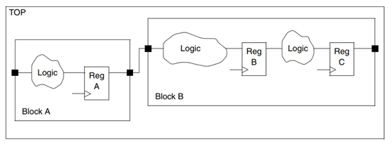
为了获得更好的结果,请避免在不同的块之间划分组合逻辑。 取而代之的是,将尽可能多的组合逻辑保持在一起,并将其与下游寄存器(如上述示例中的寄存器B)保持在一起。 必要时,在寄存器的输出(例如上述示例中的寄存器A的输出)进行分区。 这简化了低级块综合的输入和输出时序约束的设置,并为Design Compiler提供了近一个完整的时钟周期,可在其中优化寄存器到寄存器的逻辑。
在原始RTL中执行良好的分区是最佳策略。 但是,如果RTL分区不合适,则可以在编译操作之前通过取消逻辑分组并将逻辑重新分组为更有利的配置来改进Design Compiler中的分区。 默认情况下,compile_ultra命令执行自动重新分区。 您也可以使用ungroup和group命令手动重新划分设计。
For better results, avoid dividing combinational logic between different blocks. Instead, keep as much combinational logic together and keep it with the downstream registers, such as Register B in the foregoing example. Where necessary, make a partition at the output of a register, such as the output of Register A in the foregoing example. This simplifies the setting of input and output timing constraints for lower-level block synthesis and provides Design Compiler with nearly a whole clock cycle in which to optimize the register-to-register logic.
Performing good partitioning in the original RTL is the best strategy. However, if the RTL partitioning is not favorable, you can improve the partitioning in Design Compiler by ungrouping and regrouping the logic into a more favorable configuration prior to the compile operation. The compile_ultra command, by default, performs automatic repartitioning. You can also manually repartition the design with the ungroup and group commands.
路径分组
Path Groups
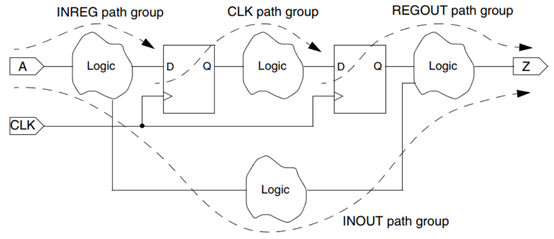
设计的时序路径被组织为称为路径组的组(不要与上一节中描述的逻辑组混淆)。 默认情况下,设计中的每个时钟都有一个路径组。 给定时钟在该路径上计时的所有时序路径
端点属于该时钟的路径组。 一个只有一个时钟的设计只有一个时钟路径组,因此设计中的所有时钟路径都属于该组。 路径组中的所有时序路径均经过优化,可以一起从关键点开始时序
路径,这是组内松弛最严重的路径。 关键路径修复后,下一条最差路径将成为新的关键路径和修复目标。 该工具将继续固定路径,直到组中的所有路径的零松弛或直到更好的优化为止
找不到当前关键路径的解决方案。 在后一种情况下,次临界路径不是固定的,但会留下时序违规。
The timing paths of the design are organized into groups called path groups (not to beconfused with logic grouping described in the foregoing section). By default, there is onepath group for each clock in the design. All timing paths clocked by a given clock at the path
endpoint belong to that clock's path group. A design that has only a single clock has only oneclocked path group, so all clocked paths in the design belong to that group. All timing paths within a path group are optimized for timing together, starting with the critical
path, which is the path having the worst slack within the group. After the critical path is fixed, the next-worst path becomes the new critical path and the target for fixing. The tool continues fixing paths until all paths in the group have zero slack or until a better optimization
solution for the current critical path cannot be found. In the latter case, the subcritical paths are not fixed, but are left with timing violations.
次临界路径是比临界路径具有更好松弛度的路径,但是仍然违反。 优化组中的路径并与其他组分开报告。 例如,在具有两个时钟CLK1和CLK2的设计中,有两个路径组。 设计编译器从最关键的路径开始,依次优化每个路径组,即使两个组之间的最差松弛时间不同。
您可以选择将路径分为几组,以控制优化工作集中在目标路径上。 例如,如果不确定输入延迟要求,则可以将输入到注册路径放入单独的组中。 在这种情况下,输入到寄存器路径与其他路径分开优化,最坏的输入到寄存器冲突并不能阻止对同一时钟提供时钟的寄存器到寄存器路径的优化。 分组路径的命令是group_path。 例如,
The subcritical paths are the paths with better slack than the critical path, but that are still in violation. Paths within a group are optimized and reported separately from other groups. For example, in a design with two clocks, CLK1 and CLK2, there are two path groups. Design Compiler
optimizes each path group in turn, starting with the critical path in each group, even if the worst slacks are different between the two groups.
You can optionally divide the paths into groups to control the focus of optimization effort on targeted paths. For example, if you are not sure about the input delay requirements, you can put the input-to-register paths into a separate group. In that case, the input-to-register paths
are optimized separately from the other paths and the worst input-to-register violation does not prevent optimization of register-to-register paths clocked by the same clock. The command for grouping paths is group_path. For example,
dc_shell> create_clock -name CLK -period 1.67 [get_ports CLK]
dc_shell> group_path -name INREG -from [all_inputs]
dc_shell> group_path -name REGOUT -to [all_outputs]
dc_shell> group_path -name INOUT -from [all_inputs] -to [all_outputs]
默认情况下,由CLK计时的路径在路径端点的所有路径都属于CLK路径组。 在此示例中,三个group_path命令将输入到寄存器路径,寄存器到输出路径和输入到输出路径分别放置在分别称为INREG,REGOUT和INOUT的单独路径组中。 寄存器间路径保留在默认的CLK组中,如图1-19所示。
By default, all paths clocked by CLK at the path endpoint belong to the CLK path group. In this example, the three group_path commands place the input-to-register, register-to-output, and input-to-output paths into separate path groups called INREG, REGOUT, and INOUT, respectively. The register-to-register paths remain in the default CLK group as demonstrated in Figure 1-19.
图1-19 时序路径分组
Figure 1-19 Timing Path Groups
使用此路径分组,在优化与输入相关或与输出相关的时序路径时遇到的任何问题都不会影响寄存器到寄存器路径的优化。 此外,report_timing命令报告每个路径组中的最差路径因此,您可以分别从输入相关路径和输出相关路径中找出最差的寄存器到寄存器路径。
With this path grouping, any problems encountered in optimizing input-related or output-related timing paths will not affect the optimization of register-to-register paths. Furthermore, the report_timing command reports the worst path in each path group
separately, so you can find out about the worst register-to-register paths separately from the input-related and output-related paths.
您可以选择为每个路径组分配一个权重,也称为成本函数,以便Design Compiler花费更多的精力来优化目标组。 每个路径组的默认权重值为1。权重越高,应用于该组的工作量就越大。 例如,以下命令与前面的示例一样分配与输入有关的路径和与输出有关的路径,但也将工作量级别指定为寄存器到寄存器路径5和2到输入到寄存器路径。 对于其他类型的路径,工作量级别保持为1。
You can optionally assign a weight, also known as cost function, to each path group so that Design Compiler applies more effort to optimizing the targeted group. The default weighting value for each path group is 1. The higher the weighting, the higher the effort applied to the group. For example, the following commands assign the input-related and output-related paths as in the previous example, but also specify an effort level of 5 for the register-to-register paths and 2 to the input-to-register paths. The effort level remains at 1 for the other types of paths.
dc_shell> create_clock -name CLK -period 1.67 [get_ports CLK]
dc_shell> group_path -name INREG -from [all_inputs] -weight 2
dc_shell> group_path -name REGOUT -to [all_outputs]
dc_shell> group_path -name INOUT -from [all_inputs] -to [all_outputs]
dc_shell> group_path -name CLK -weight 5
一个组若拥有较高的权重意味着Design Compiler将尝试减少该组中路径的时序违规的大小,但代价是属于较低权重组的路径的松弛。 要获取有关当前路径组集的信息,请使用report_path_group命令。 要删除路径组,请使用remove_path_group命令。 属于已删除组的路径被隐式分配给默认路径组。
Higher weighting for a group means that Design Compiler will attempt to reduce the size of a timing violation for a path in that group at the expense of slack in a path belonging to a lower-weighted group. To get information about the current set of path groups, use the report_path_groupcommand. To remove a path group, use the remove_path_group command. Paths belonging to a removed group are implicitly assigned to the default path group.
寄存器时序再优化
Register Retiming Optimization
满足时序约束的另一种方法是在组合逻辑内重新放置寄存器。 例如,在图1-20中,由于较长的组合逻辑路径,左侧的时序路径违反了设置时序,该路径的总时间裕量为–1.0。 同时,下游的短时间路径拥有一个+1.5的时间裕量。
Another way to meet timing constraints is to reposition registers within the combinational logic. For example, in Figure 1-20, the timing path on the left has a setup timing violation due to a long combinational logic path, with a total slack of –1.0 for the path. Meanwhile, the short timing path downstream has a positive slack of +1.5.
图1-20 建立时间违例
Figure 1-20 Setup Timing Violation
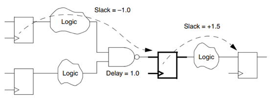
Design Compiler可以通过更改实现来解决此冲突,如图1-21所示。 它会取走"与非"门输出处的寄存器,并用同一"与非"门的输入处的两个新寄存器代替它。 这产生了一个逻辑上等效的电路,该电路通过了两条路径的建立时序。 该改变有效地消除了来自违反路径的NAND门的延迟,并将该延迟提供给下游路径。 这种定时违规校正的成本是电路中附加寄存器的面积。
Design Compiler can fix this violation by changing the implementation as shown inFigure 1-21. It takes away the register at the output of the NAND gate and replaces it with two new registers at the inputs of the same NAND gate. This produces a logically equivalent circuit that passes setup timing for both paths. The change effectively takes away the delay of the NAND gate from the violating path and gives that delay to the downstream path. The cost of this timing violation correction is the area of the additional register in the circuit.
图1-21 通过寄存器时序调整修复违例
Figure 1-21 Violation Fixed by Register Retiming
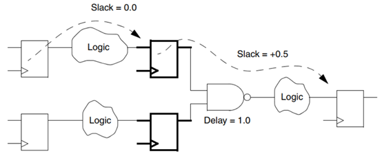
相反,如图1-21所示的电路,但在第一时序路径中有一些可用的时序裕量,可以通过取下与非门输入处的两个寄存器并用一个代替单个寄存器来减小总面积。 在与非门的输出处注册。通过拆分或合并寄存器并通过组合逻辑移动这些寄存器(无论是为了获得更好的时序还是达到更好的面积)而进行的优化称为寄存器重新定位或寄存器重新计时。 这种类型的优化是通过命令compile_ultra -retime,balance_registers或optimize_registers执行的。
Conversely, a circuit like the one shown in Figure 1-21, but with some available timing slack in the first timing path, can reduce the total area by taking away the two registers at the inputs of the NAND gate and replacing them with a single register at the output of the NAND gate.
Optimization performed by splitting or merging registers and moving those registers through combinational logic, whether for better timing or better area, is called register repositioningor register retiming. This type of optimization is performed with the commandcompile_ultra -retime, balance_registers, or optimize_registers.