Turn-off time less than 2μs
Max. operating frequency greater than 500kHz
Temperature stability of 0.005% per °C
PIN Configuration
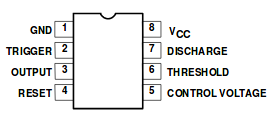
Pin1 GND 地线(或共同接地), 外接电源负端VSS或接地, 一般情况下接地
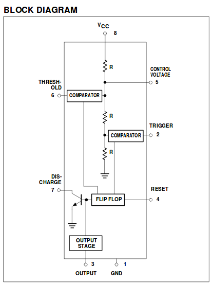
Pin2 TRI Trigger 低触发端, 这个脚位是触发NE555使其启动它的时间周期, 触发信号上缘电压须大于2/3 VCC, 下缘须低于1/3 VCC A low voltage (less than 1/3 the supply voltage) applied momentarily to the Trigger input causes the output (pin 3) to go high. The output will remain high until a high voltage is applied to the Threshold input (pin 6).
Pin3 OUT Output 输出端Vo, 时间周期开始时移至比电源电压低1.7V的高电位, 周期结束时输出回到OV左右的低电位, 高电位时的最大输出电流大约200mA. In output low state the voltage will be close to 0V. In output high state the voltage will be 1.7V lower than the supply voltage. For example, if the supply voltage is 5V output high voltage will be 3.3 volts. The output can source or sink up to 200 mA (maximum depends on supply voltage)
Pin4 RES Reset 直接清零端, 低逻辑电位送至这个脚位时会重置定时器, 使输出回到一个低电位. 当此端接低电平时, 时基电路不工作,此时不论TR, TH处于何电平, 时基电路输出低电位. 该端不用时应接高电平
Pin5 CON Control Voltage 控制电压端, 若此端外接电压, 则可改变内部两个比较器的基准电压, 这个可以小范围调节稳态时的脉冲长度或非稳态时的频率. 当该端不用时应将该端串入一只0.01μF电容接地, 以防引入干扰. 这个接脚准许由外部电压改变触发和闸限电压, 当计时器经营在稳定或振荡的运作方式下, 这输入能用来改变或调整输出频率. You can control the threshold voltage (pin 6) through the control input (which is internally set to 2/3 the supply voltage). You can vary it from 45% to 90% of the supply voltage. This enables you to vary the length of the output pulse in monostable mode or the output frequency in astable mode. When not in use it is recommended that this input be connected to circuit ground via a 0.01uF capacitor.
Pin 5 is control, you can control the operation of the timer from an outside source. The Control is often used for audio modulation, but for a simple square wave generator it is usually not used. However, if you leave the pin unconnected, it can pick up electromagnetic waves that can cause a tiny bit of erratic behavior, which is often undesired. If you're only using the chip to flash an LED, for example, you probably don't need the capacitor. You probably won't see the difference. The .01uF cap is only there to eliminate the unwanted signals.
Pin6 TRE Threshold 高触发端, 重置锁定并使输出呈低态. 当此pin的电压从低于1/3VCC移至高于2/3VCC时启动这个动作 In both astable and monostable mode the voltage across the timing capacitor is monitored through the Threshold input. When the voltage at this input rises above the threshold value the output will go from high to low.
Pin7 DIS Discharge 放电端, 该端与放电管集电极相连, 用做定时器时电容的放电. 这个接脚和输出脚有相同的电流输出能力, 当Pin3为低电平时, Pin7对地为低阻态(对地导通), 当Pin3为高电平时, Pin7对于为高阻态 when the voltage across the timing capacitor exceeds the threshold value. The timing capacitor is discharged through this input
Pin8 VCC 正电源电压端, 外接电源VCC,双极型时基电路VCC的范围是4.5~16V, CMOS型时基电路VCC的范围为3~18V. 一般用5V供应.
应用电路1: Astable Operation 非稳态电路(多谐振荡器)
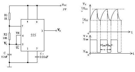
多谐振荡器又称为无稳态触发器, 没有稳定的输出状态, 只有两个暂稳态. 在电路处于某一暂稳态后, 经过一段时间可以自行触发翻转到另一暂稳态. 两个暂稳态自行相互转换而输出一系列矩形波. 多谐振荡器可用作方波发生器.
接通电源后, 输出假定是高电平,则Pin7截止, 电容C充电. 充电回路是VCC - R1 - R2 - C - GND, 按指数规律上升, 当上升到2/3 VCC时(Threshold端电平大于Vc), 输出翻转为低电平. Vo是低电平, Pin7导通, C放电, 放电回路为C - R2 - T - GND, 按指数规律下降, 当下降到1/3 VCC时(Threshold端电平小于Vc), 输出翻转为高电平, 放电管T截止, 电容再次充电, 如此周而复始, 产生振荡.
输出高电平时间 T = (R1 + R2) * C * ln2
输出低电平时间T = R2 * C * ln2
振荡周期 T = (R1 + 2R2) * C * ln2
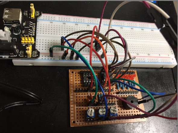
使用面包板和测试板对上面电路的测试. 用一个104(100k)的电位器代替R2, 测试不同的R2值下蜂鸣器的声音. 在R2在0~10K范围时, 是一种清脆的"滴"声, 在大于50K之后声音越来越闷, 逐渐接近于漏电时急促的"嗒嗒嗒"声.
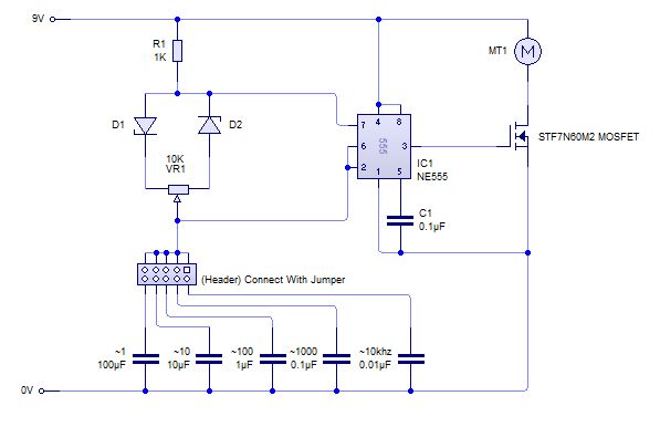
应用电路2: Less Than 50% Duty Cycle Astable MultivibratorAstable
前一个电路的占空比只能在55%~100%之间调节, 下面是改进的电路, 可以让占空比在 9%~100% 之间调节. 通过两个1N4148二极管控制充放电时的电流流向, 当电位器触点靠左时, 充放电的时间比为1:10, 占空比为1/11约9%, 在靠右时, 充放电的时间比为11:0, 占空比为100%. 通过下方的电容容量切换, 可以显著调节输出的频率.