接口速度:
| type | bw | |
| read | 75μs | 1s/75μs*8k/1s=104m/s |
| write | 1300μs | 1s/1300μs*8k/1s=6m/s |
| erase | 3.8ms | 1s/3.8ms*8k*256/1s=526m/s |
| PCIe Gen2 x8 | 5Gbps | 5Gbps/8*8=4.88G/s |
| DDR3 | 533MHz(32bit) | 32bit*533MHZ/8=2.132GB/s |
|
system bus- AXI-Lite (bus 32 bits) |
Used for control Operates @ 100MHz |
|
|
storage data bus- AXI (bus 64 bits, burst length: 16) |
Used for DMA operations between flash storage controller/PCIe interface and DRAM Operates @ 100 MHz |
64bit*100MHZ/8=800m/s |
| flash bus | Operates @ 50MHz, DDR (100MB/s data rate) | 8bit*50MHZ/8=50m/s |
数据传输
PCIE <--DMA--AXI--> DRAM <--DMA--AXI> FSC <--flash bus--> DIE
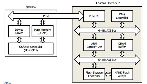
FSC控制器结构如下:
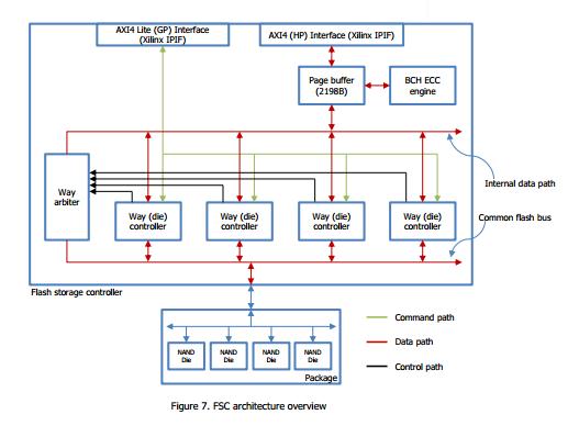
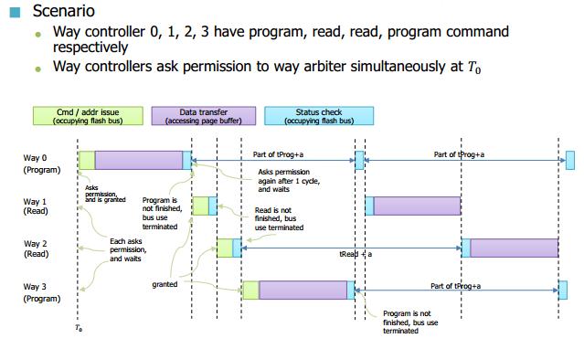
Way arbiter
Way arbiter是用在当有多个way controller都要请求commonflash bus 和 access page buffer,因为是公用的,所以就要分配permission权限,算法如下:
lastGrantedWay = 0
while (true)
if (requestArrived)
for (i = 0 to numberOfWays)
nextCandidate = (lastGrantedWay + i) % numberOfWays //就是从上次使用的way继续往下轮训着找
if (hasRequested(nextCandidate))
grantPermission(nextCandidate)
permission权限的意思是指(每次只有一个way可以使用):
● Access page buffer (through data path)
● Use flash bus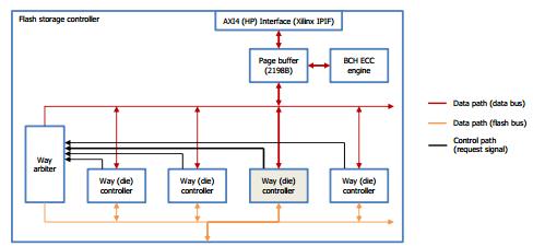
下面列出一个example:
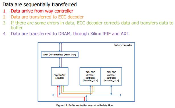
Buffer controller
Buffer controller controls data bus between page buffer and BCH ECC encoder/decoder
Buffer size is 2198B
● Data 2048B + 60B ECC parity + reserved (90B)
– Reserved space was intended to support more powerful ECC (currently not used)
● Page size of flash device is 8192B, thus, data transfer occurs 4 times
写过程:

读过程:
page结构
1.Physical page size of flash device
■ 8KB+448B (8640B)
2.There are four chunks
■ Each chunk consists of a pair of data and parity
3.Reserved 40B area is intended to store FTL metadata (currently not used)

way controller
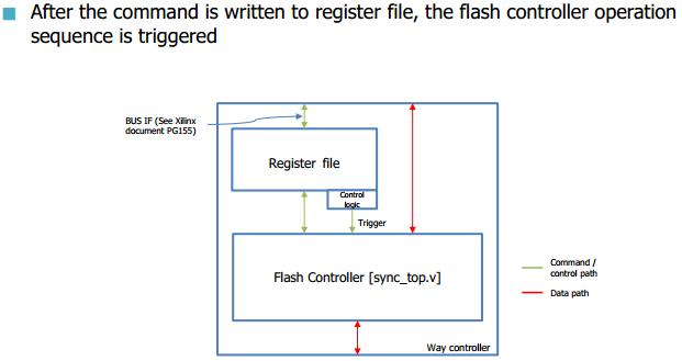
下面来看flash controller的具体结构:
①Reset, mode change commands are directly executed at their dedicated modules
● Reset module and mode change module are responsible for the control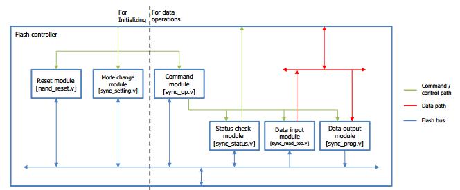
②Page read, page program, block erase commands are executed in 2-3 stages