在之前的“Xilinx 7系列FPGA部分重配置【1】”中已经较为详细地记录了分别在工程模式(Project Mode)和非工程模式(Non-Project Mode)下、使用7系列的Xilinx FPGA芯片创建部分重配置(Partial Reconfiguration,PR)项目、并生成相应的bit配置文件的流程。
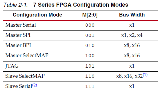
前述流程是一个较为基本的PR项目操作流程、在UG947和UG909文档的示范例中都有说明,自己也按照前述的流程、参考UG文档、在Xilinx Arty评估板上(xc7a35ticsg324-1L)创建了两个简单的PR项目、对PR功能成功进行了实现和验证。评估板上的下载和调试接口是USB JTAG,对FPGA的下载和配置使用的是JTAG模式。根据UG470,FPGA的配置模式主要包含以下几种:
在粗略地整体浏览完UG470之后意识到,JTAG模式是一种健壮性相对比较好的配置模式。
而前段时间工作项目上、板上FPGA的型号为xc7a35tftg256-1、配置模式为从串模式、FPGA的配置文件由另外一个stm32芯片进行加载,并且整个PR项目的复杂度远非UG文档上的示例所可比拟(由于实际应用的需求,接手的FPGA工程的复杂度主要体现在user IO的使用率极高、几乎用完了全部可分配的管脚),所以按照前述PR项目的创建和配置文件生成流程进行操作之后、一直无法通过PR验证。
后来在仔细参考了当前项目之前的降级版本的项目片上FPGA的工程文件包之后、在VIVADO的批处理模式下(batch mode)、运行编写的TCL脚本、使用和之前一样的代码包作为源文件、重新生成了FPGA配置文件,在测试板上实验之后、PR功能验证通过。所以在这里将TCL脚本中、相对前述的操作流程作出更改的几个点进行记录,以便日后参考。
1、设计思路改变
自己在之前的PR操作中一直采取的思路是:
begin
分别生成顶层的逻辑综合dcp(末尾有RP(Reconfigurable Partition)黑盒子定义)、以及N种RM的综合dcp-
使用顶层+RM1拼接生成第一种全局配置-
挖空RP(updata_design -black_box)得到static.dcp-
打开static.dcp-
填入第二种RM-
实现第二个全局配置-
……
填入第N种RM-
实现第N个全局配置
end
而参考了前人的TCL脚本之后、现在采取的创建思路是:
begin
直接利用全部的.v文件生成第一种完整的配置(TOP.v文件末尾不包含对RP的黑盒子定义)-
将RP挖空(updata_design -black_box)、得到static.dcp-
综合第二中RM、执行reset_timing命令、保存为RM_2nd.dcp
填入第二种RM-
实现第二个全局配置-
……
填入第N种RM-
实现第N个全局配置
end
需要注意的是,在保存生成的第二个RM的综合dcp之前进行了一个reset_timing的命令,这在之前做的时候都是没注意过、也没采用过的。
2、综合命令选项
执行synth_design时需要指定的属性变量
如果对A模块做综合时、B模块中的参数需要通过A模块传递过去,那么在综合时可以使用-generic属性,格式如下:
-generic <name>=<value> - (Optional)
The value of a VHDL generic entity, or of a Verilog parameter. The -generic option can be used to override the assigned values of parameters in the RTL design sources. However it can only override parameters at the top level of the design. Repeat the -generic option multiple times in the synth_design command for each generic or parameter value to be defined.
在进行PR项目中还进行设置了的属性包括
-flatten_hierarchy <arg> - (Optional)
Flatten the hierarchy of the design during LUT mapping. The valid values are:
* rebuilt - This will attempt to rebuild the original hierarchy of the
RTL design after synthesis has completed. This is the default setting.
* full - Flatten the hierarchy of the design.
* none - Do not flatten the hierarchy of the design. This will preserve
the hierarchy of the design, but will also limit the design optimization that can be performed by the synthesis tool.
设计中指定的是none。
-no_lc - (Optional)
Disable the default LUT combining feature of Vivado synthesis.
设计中使用了-no_lc。
-fsm_extraction <arg> - (Optional)
Finite state machine (FSM) encoding is automatic (auto) in Vivado synthesis by default. This option enables state machine identification and specifies the type of encoding that should be applied. Valid values are: off, one_hot, sequential, johnson, gray, auto.
设计中指定的是off
综合后续RM时还指定了OOT模式。
-mode [ default | out_of_context ] - (Optional)
Out of Context mode specifies the synthesis of an IP module, or block module, for use in an out-of-context design flow. This mode turns off I/O buffer insertion for the module, and marks the module as OOC, to facilitate its use in the tool flow. The block can also be implemented for analysis purposes. Refer to the Vivado Design Suite User Guide: Designing with IP (UG896) or the Vivado Design Suite User Guide: Hierarchical Design (UG905) for more information.
3、布局布线、实现命令选项
执行place_design命令时需要指定的属性变量:
-directive <arg> - (Optional)
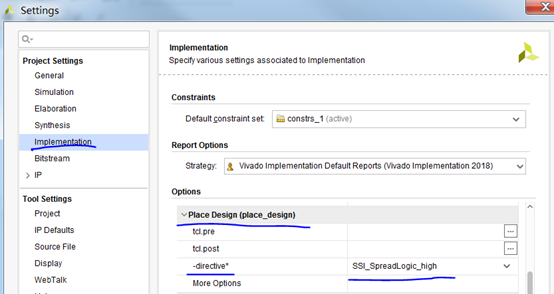
Direct placement to achieve specific design objectives. Only one directive can be specified for a single place_design command, and values are case-sensitive.
* SSI_SpreadLogic_high - Distribute logic across SLRs. SSI_SpreadLogic_high achieves the highest level of distribution.
* SSI_SpreadLogic_low - Distribute logic across SLRs. SSI_SpreadLogic_low achieves a minimum level of logic distribution, while reducing placement runtime.
还可以为该-directive属性指定其它很多种值、这里没有一一列举,设计中指定的是SSI_SpreadLogic_high
在执行最后一步的write_bitstream命令之前需要进行的设定包括:
set_property CONFIG_MODE S_SERIAL [current_design]
set_property BITSTREAM.CONFIG.PERSIST Yes [current_design]
set_property BITSTREAM.SEU.ESSENTIALBITS YES [current_design]
set_property BITSTREAM.GENERAL.COMPRESS TRUE [current_design]
其中第三条根据字面意思是增强FPGA的SEU方面性能的设定、未在UG文档中找到相应说明,其余语句的含义依次如下:
set_property CONFIG_MODE S_SERIAL [current_design]
设定FPGA的配置模式为从串
set_property BITSTREAM.CONFIG.PERSIST Yes [current_design]
为FPGA的配置添加全局PERSIST属性
set_property BITSTREAM.GENERAL.COMPRESS TRUE [current_design]
选择在生成bit配置文件时进行压缩处理、提高生成速度
其中的第二条语句,查阅UG908可以看到:
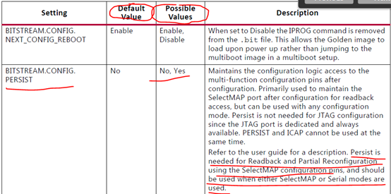
根据其大意,该参数默认值为no,在进行PR项目、配置模式为串行等情况下需要将该参数设置为yes。
在UG470中对persist option的说明如下(P128):
The persist bitstream option maintains the configuration logic access to the multi-function configuration pins after configuration. The persist option is primarily used to maintain the SelectMAP port after configuration for readback access. Persist is not needed for JTAG configuration since the JTAG port is dedicated and always available. Persist and ICAP cannot be used at the same time. PERSIST is also not recommended for standard Master SPI/BPI configuration mode setups. For advanced tandem Master SPI/BPI configuration mode setups refer to XAPP1179, for the PERSIST option usage.
The persist option can also be used to reconfigure the device from an external controller without pulsing the PROGRAM_B pin or using the JTAG port. The multi-function pins that persist depend on the configuration mode pin settings, and are the same as those shown for each configuration mode in Table 2-2, page 22 and Table 2-3, page 23, except that PUDC_B and DOUT_CSO_B never persist. Any I/O pins that persist cannot be used as I/O in the user design. Use the CONFIG_MODE constraint to reserve the correct pins during implementation of the design. Persisted I/O use the general-purpose I/O standard default of LVCMOS, 12 mA drive, Slow slew rate.
4、意外错误记录
(1)BITSTREAM.CONFIG.PERSIST设置和7系列FPGA芯片的RS[1:0]管脚相关
在执行上述第三点最后的“set_property BITSTREAM.CONFIG.PERSIST Yes [current_design]”语句之后、执行write_bitstream命令之后报错,显示不能为项目中的某一个引脚添加该PERSIST属性、当把项目中使用到该引脚的代码、以及该引脚对应的约束文件行删掉之后,write_bitstream命令顺利执行。具体到当前项目,使用的FPGA型号为xc7a35tftg256-1、出现错误提示的引脚号为H14(以及G15)。
查阅对应的芯片管脚封装手册UG475可以看到,这两个脚在封装图里面的小方块中标记为r,如下图:
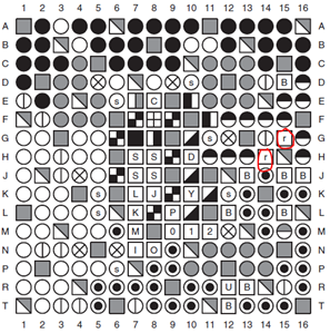
UG475文档结合UG470对r的注释为:
|
Pin Name |
Type |
Direction |
Description |
|
RS0 or RS1 |
Multi-function |
Output |
The RS0 and RS1 pins are revision selection output pins,intended to drive upper address lines on a parallel flashmemory. Normally, RS0 and RS1 are high-Z duringconfiguration. However, the FPGA can drive the RS0 and RS1 pins under two possible conditions. When theConfigFallback option is enabled, the FPGA drives RS0and RS1 Low during the fallback configuration processthat follows a detected configuration error. When auser-invoked MultiBoot configuration is initiated, the FPGA can drive the RS0 and RS1 pins to a user-defined state during the MultiBoot configuration process. If fallback is disabled (default) and if MultiBoot is notused, or if SPI mode is used, then RS0 and RS1 are high-Z and can be left unconnected. |
在UG470中对这两个脚的说明是:
RS0 and RS1 are only driven when a MultiBoot event is initiated or when the ConfigFallback option is enabled and a Fallback event occurs.
Otherwise, RS0 and RS1 are high-Z. When using the RS[1:0] pins for configuration it is recommended not to use them in User mode.
P62:
RS[1:0] are typically high impedance. However, a MultiBoot (or Fallback event in BPI mode) can cause RS[1:0] to drive High or Low.
P145:
RS Pins
The dual-purpose RS pins are disabled by default. The RS pins drive Low during a fallback for BPI or Master SelectMAP mode, but do not drive Low during SPI mode. For initial MultiBoot systems, the RS pins are wired to upper address bits of the flash and strapped High or Low with a pull-up or pull-down resistor, respectively. At power up, the system boots to the upper address space defined by the pull-up resistors on the RS and address line connections. During a fallback, the RS pins drive Low and the device boots from address space 0. The RS pins should be tied to upper addresses defined by the system to allow for full bit files to be stored in each memory segment.
P146:
In all configuration modes except SPI mode, RS[1:0] is controllable by WBSTAR.
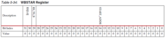
在P119中讲到了WBSTAR相关的内容,也涉及到了RS[1:0],具体如下所示:
The warm boot start address register (WBSTAR) specifies the MultiBoot address location to be used when the IPROG command is applied. The name of each bit position in the warm boot start address register is given in Table 5-34 and described in Table 5-35.

讲解PR的UG908(v2018.2)的P118中提到:
To use external configuration modes (other than JTAG) for loading a partial BIT file, these pins must be reserved for use after the initial device configuration. This is achieved by using the BITSTREAM.CONFIG.PERSIST property to keep the dual-purpose I/O for configuration usage and to set the configuration width. Refer to this link in the Vivado Design Suite User Guide: Programming and Debugging (UG908) [Ref 25]. The Tcl command syntax to set this property is:
set_property BITSTREAM.CONFIG.PERSIST <value> [current_design]
where <value> is either No or Yes.
按照个人理解、这段话中所指的'these pins'指的是在UG470的Table2-2和Table2-3中列出的全部Configuration Pins、其中就包含RS0 和RS1 pins(属于Multi-function pins也就是dual-purpose pins)。
而在一般的用于成熟的商用产品的设计中、显然也会经常用到除了JTAG之外的、对FPGA进行配置的配置模式。
根据上述信息、为确保安全起见、在设计PR项目的FPGA硬件电路时、应当避免将具体芯片的RS0 和RS1管脚作为普通IO引脚使用(前提当然是选用的具体型号的FPGA芯片上包含这两个引脚)。
(2)TCL脚本相关-VIVADO的shell模式和batch模式
之前在VIVADO的非工程模式下进行PR项目的工作时、不管是直接在windows的命令提示符窗口还是VIVADO GUI下的TCL Console,使用的都是shell模式的vivado,而后来仿照前人项目进行工作时、都是在windows的命令提示符窗口进入vivado的batch模式、使用source语句(vivado -mode batch -source <your_Tcl_script>)运行编写好的tcl脚本。
在进行工作期间发现、当综合同样一个顶层模块时,
方式一:
在vivado的batch模式下运行编写好的tcl脚本,tcl的脚本内容依次大致为:
read_verilog <file_name1.v>

read_verilog <file_name2.v>

...

read_xdc <xdc_file.xdc>

synth_design -no_lc ... ...
方式二:
使用和方式一相同的.v和.xdc源文件、在vivado的shell模式下(不管是命令提示符窗口还是VIVADO GUI Tcl Console),一行一行的敲进去方式一中脚本文件内的命令,然后一条一条地执行。
这两种方式运行完了之后,VIVADO给出的提示不尽相同;并且如果都只是warnings还好,问题就出在,在某些时候,方式一的结果会报出error、但同时synth_design是显示成功执行了的(error在Tcl Console中也找不到、但是就是显示有1 error),而方式二却不会报出error。
这个问题可能是由于vivado shell mode和batch mode工作时的细微差别所致,具体原因尚不明,仅记录在此,供日后参考。
5、额外注意点
(1)在做Floorplan步骤中、绘制Pblock的注意点
根据UG947和UG909,在综合之后、为每个RP的instance绘制相应的Pblock时,需要注意的基本点包括:
一般需要将RESET_AFTER_RECONFIG设置为TRUE(默认为FALSE);
一般需要将SNAPPING_MODE设置为ROUTING(或者设置为ON,默认为OFF);
当使用RESET_AFTER_RECONFIG的情况下,需要让绘制的Pblock的垂直方向上的两个边界与clock region的垂直边界对齐;
确保绘制的Pblock中所包含的逻辑资源是足够的(为当下的布局布线和后续RM可能的升级修改留出足够空间)。
除了上述注意点之外,目前找不到更多的明确提出了的注意点。
如下图所示是xc7a35tftg256-1型号FPGA的VIVADO下的Device页面:
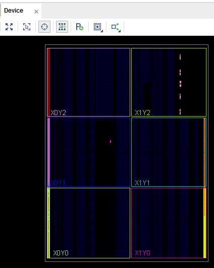
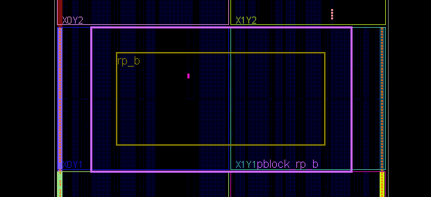
可以看到其中包含6个clock region。之前在做PR工程期间,只敢让一个RP的Pblock占据一个clock region,而在查阅UG文档、以及借鉴了前人的PR项目案例之后,发现可以让一个RP的Pblock占据多个clock region,比如可以是下图这样:
也似乎可以是下图这样(来自UG909-P87-Fig.6-1):
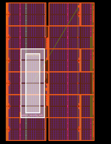
所以根据目前的有限了解,不需要将一个RP的Pblock局限在一个clock region之中。
(2)PR项目的工程和非工程模式
由于在开始接手PR项目任务时、在开始阶段一直在工程模式下操作,所以在使用Tcl脚本(非工程模式)生成了可以通过PR测试的配置文件、交差之后,(抱着Project Mode不死心的态度)又在工程模式下新建了项目、按照Tcl脚本中对一些关键命令的属性参数设置修改了工程模式下的一些属性设置,分别如下所示。
综合设置:

Implementation设置:
在打开open implementation之后、write bitstream之前进行的设置:
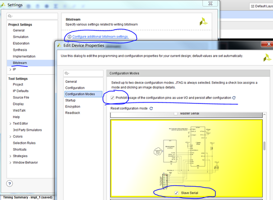
这里上面打钩的“Prohibit usage of……”设置其实就是设置了BITSTREAM.CONFIG.PERSIST Yes的属性,在UG702中也找到了对该点的说明(虽然UG702是针对ISE的):
-g Persist:Yes
Prohibits the use of the dual-purpose configuration pins as user I/O, which is required if Slave SelectMAP or Slave Serial modes are to be used for Partial Reconfiguration. This option should be used in conjunction with the CONFIG_MODE constraint to select the proper set of configuration pins to be reserved for post-configuration use. Consult the Constraints Guide (UG625) for the complete set of values for CONFIG_MODE (examples: S_SELECTMAP, S_SERIAL).
为了提高速度也设置了bit压缩:

工程模式的project下、RM等的添加和之前操作流程没有变化,都是通过partial configuration wizard下管理和添加(见上一篇PR)。
按照这样的设置、继续使用了tcl脚本模式下的pblock区块规划。
使用这样在Project Mode下生成的bit配置文件、打包下载到电路板上,也成功通过了PR测试!
总结来看:在vivado batch mode的非工程模式下使用TCL脚本和在VIVADO GUI下全程通过工程模式,都可以创建出满足PR需求的bit配置文件,关键主要在于synth_design、place_design和write_bitstream等关键步骤中重要属性参数的设置。