Tensor Processoring Unit
TPU V1 2015
- 2CH的2133MHz的DDR3内存是Off Die的,一共8GiB;
- 内存的带宽:2Channel*2133MHz*64bit/8/1000=34GB/s
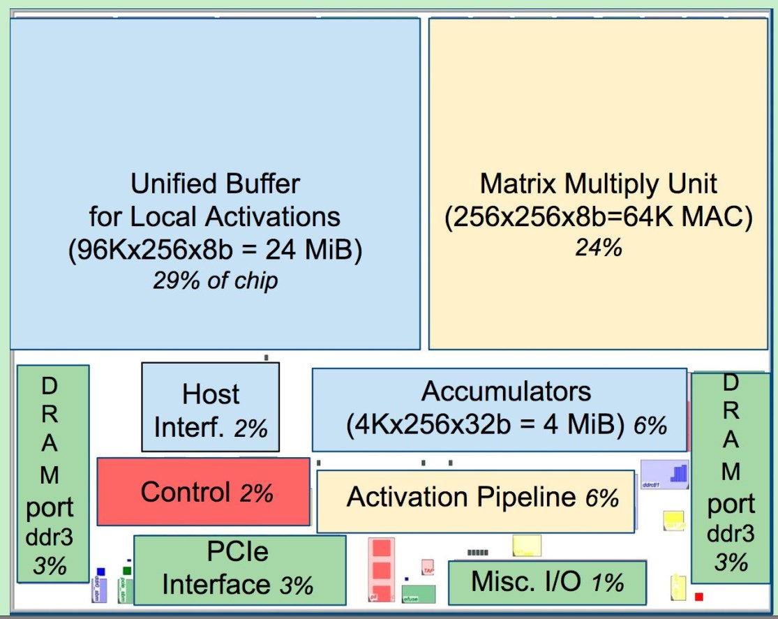
- 256*256=65536 8bit MAC 矩阵乘法单元
- 700MHz,Peak :65536*2(M/A)*700MHz=92T INT8 Operations/second
- 28MiB的片上内存
- 4MiB的加法器内存
- 24MiB的统一Buffer;
- 下面是个透视图
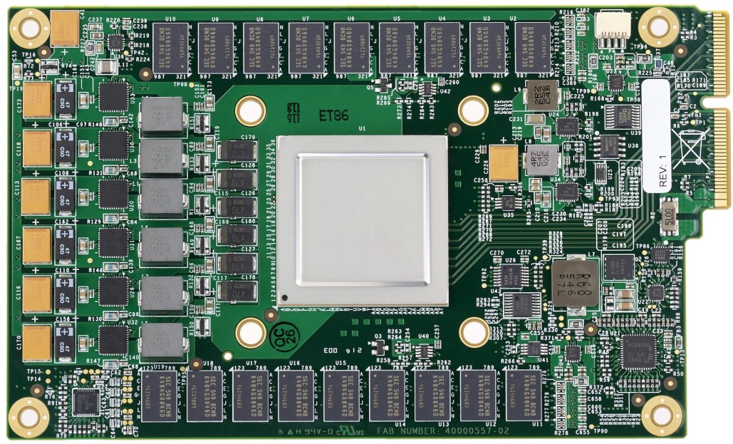
- TPU组成的加速卡,每个服务器上放4个;
TPU V2 2017
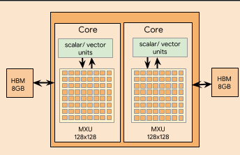
TPU V2 Chip Block Diagram
TFLOPs:
1 MXU Per Core
22.5TFLOPs Per core , 8GB HBM Per Core;2 Cores per chip, means 45 TFLOPs per Chip4 Chips per board, means 180TFLOPs per BoardMostly fp32
Mrtaix Unit:
128*128 array; float32 accumulate, bfloat16 multiplies;
就是矩阵式脉动阵列的一种,权重不变,输入X,输出Y;
内存带宽,不知道内存的位宽和频率。
TPU V2 Board (V2-8)(一个板子上有四个芯片,每个芯片两个Core)

Connect to Host CPU through 32 Lans PCIe Gen3
180 Teraflops of computation
64GB of HBM Memory
2400GB/s memory BW
TPU V2部署的机房:
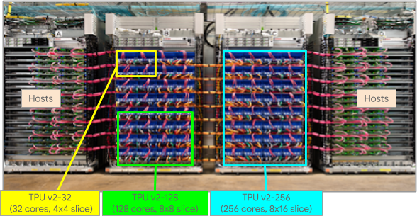
TPU V2 可以形成的最大的Pod (V2-8*64-512)(一个池子有64块板子,左边32个,右边32个)

64 pic of V2 Board,64*8=512个TPU V2 Core;
11.5 pflops of computation
4TB of HBM Memory
2D torus 环形 topology
TPU V3 2019
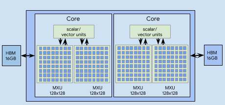
TPU V3 Chip Bloack Diagram
TFLOPs:
?? TFLOPs Per core , 16GB HBM Per Core;2 MXU Per Core2 Cores per chip,4 Chips per board,Mostly fp32
Mrtaix Unit:
输入和输出都是FP32,但是乘法运算是按照BF16进行计算的;
128*128 array; float32 accumulate, bfloat16 multiplies;
就是矩阵式脉动阵列的一种,权重不变,输入X,输出Y;
TPU V3 Board(V3-8)(一个板子上有四个芯片,每个芯片两个Core)
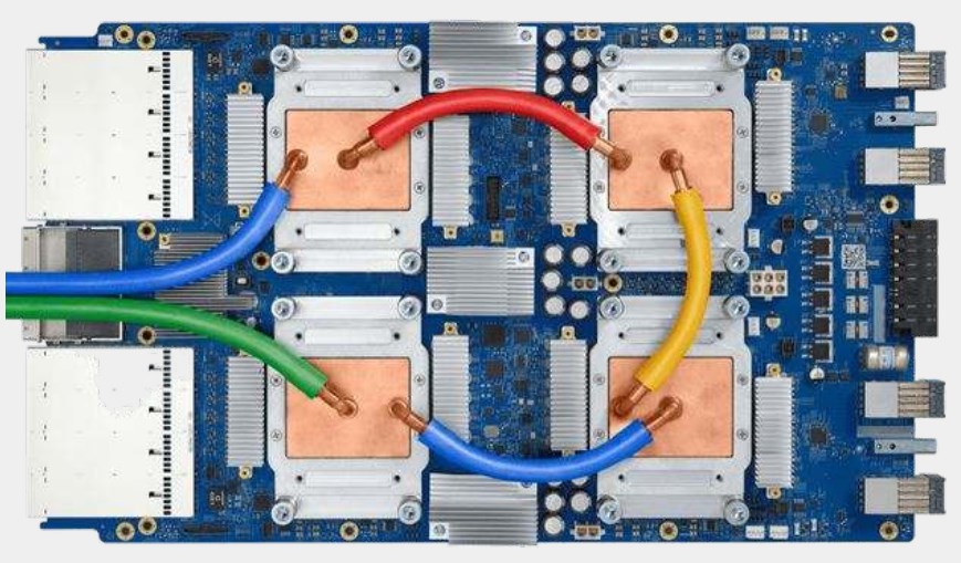
420Teraflops of computation,乘法还是BF16,但是输入和输出还是TF32的。
128GB of HBM Memory
Liquid Cooling
TPU V3部署的机房:
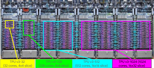
TPU V3可以形成的最大的 Pod(V3-8*256-2048)(一个池子256个板子,256*8Core=2048Core,上面8个机柜共同组成最大的Pod)
Over 100 pflops
32TB of HBM Memory;
参考文献:
2017年HotChip上第一次介绍TPU V1:https://www.hotchips.org/archives/2010s/hc29/ HC29.22.730-TensorPU-Young-Google.pdf
2017年在ISCA发布的第一代的TPU的论文:https://arxiv.org/ftp/arxiv/papers/1704/1704.04760.pdf
2019年HotChip上的培训:https://www.hotchips.org/hc31/HC31_T3_Cloud_TPU_Codesign.pdf
最后Cloud TPU的地址:https://cloud.google.com/tpu