报错一:
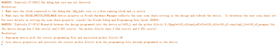
WARNING: [Labtools 27-3361] The debug hub core was not detected.
Resolution:
1. Make sure the clock connected to the debug hub (dbg_hub) core is a free running clock and is active.
2. Make sure the BSCAN_SWITCH_USER_MASK device property in Vivado Hardware Manager reflects the user scan chain setting in the design and refresh the device. To determine the user scan chain setting in the design, open the implemented design and use 'get_property C_USER_SCAN_CHAIN [get_debug_cores dbg_hub]'.
For more details on setting the scan chain property, consult the Vivado Debug and Programming User Guide (UG908).
WARNING: [Labtools 27-1974] Mismatch between the design programmed into the device xc7z020_1 and the probes file(s) E:/fpga/mt100_v2/nand_x8/v2/mt100_v2/mt100_v2.runs/impl_1/mt100_v2_wrapper.ltx.
The device design has 0 ILA core(s) and 0 VIO core(s). The probes file(s) have 3 ILA core(s) and 0 VIO core(s).
Resolution:
1. Reprogram device with the correct programming file and associated probes file(s) OR
2. Goto device properties and associate the correct probes file(s) with the programming file already programmed in the device.
报错二:
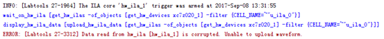
ERROR: [Labtools 27-3312] Data read from hw_ila [hw_ila_1] is corrupted. Unable to upload waveform.
首先要了解什么是 debug hub core?
a debug core hub (dbg_hub) is automatically inserted into the synthesized design netlist to provide connectivity between the new ILA core and the JTAG scan chain.
debug hub 负责将一个或几个ILA与JTAG连接起来。JTAG指令下发以及抓取的波形数据回传到screen都要通过它。
(参考 p133 - ug908-vivado-programming-debugging.pdf)
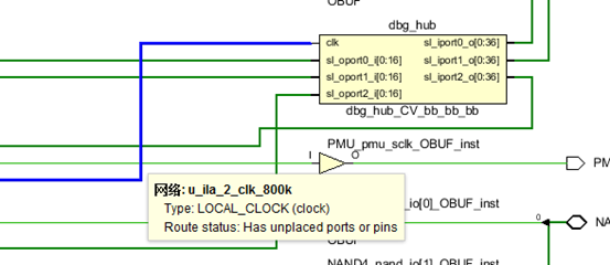 就像这个,把3个ILA连到JTAG上。
从warning的提示来看,1、这个hub的clock不正常;或者2、两个参数不匹配(一般参数都是01没问题,可以在properties中查到)。
那么重点是clk为什么不对?
Make sure the clock connected to the debug hub (dbg_hub) core is a free running clock and is active.
我遇到过两种情况,导致clock不正常的。
1、clock线连上了,但是这个wire上却没有clock波形,因为zynq的ps端没有启动配置,所以没有任何clock到pl端;
2、我们设置的clock频率跟JTAG仿真器的不匹配。重点来说这个。
在之前正常的project中,dbg_hub的clk都是连接在clk_out1(40mhz)上,这次连到了clk_800k,为什么连接变了? 频率低了有什么问题?
在p35-ug908上有指明 “The JTAG chain is as fast as the slowest device in the chain.”
dbg_hub上面一共挂了3个device,clock分别是40mhz、20mhz、800khz,所以才连到了这个最低的800k上面。
在xilinx的forum上有个QA,Data read from hw_ila is corrupted 。其中提到 “Can you please check whether your JTAG frequency is lower than ILA clock frequency? It is recommended to keep the JTAG frequency half or less than half of ILA clock frequency.”
虽然后半句,推荐一半或更低的freq没有在ug908上找到依据,但是jtag比ILA低这个是原理性的。The JTAG chain is as fast as the slowest device in the chain.也是这个意思。

ERROR: [Xicom 50-38] xicom: No trigger mark in any sample in window: 0.
ERROR: [Xicom 50-41] Waveform data read from ILA core is corrupted (user chain=1, slave index=0).
Resolution:
1) Ensure that the clock signal connected to the debug core and/or debug hub is clean and free-running.
2) Ensure that the clock connected to the debug core and/or debug hub meets all timing constraints.
3) Ensure that the clock connected to debug core and/or debug hub is faster than the JTAG clock frequency.
ERROR: [Xicom 50-38] xicom: Error during interpreting trace readback data
ERROR: [Labtools 27-3176] hw_server failed during internal command.
Resolution: Check that the hw_server is running and the hardware connectivity to the target
这次报错已经说明的很清楚了,ILA和HUB的clock一定要比JTAG的高!
p35上还有一段,”a default JTAG clock frequency that is 15 MHz for the Digilent cable connection and 6 MHz for the USB cable connection.“
也就是说,我用的这个USB-JTAG仿真器跑的默认频率是6mhz。这个6mhz比40mhz和20mhz低可以work,但明显高于800k的。
那么根因已经很清楚了,报错的project中debug hub这个中间连接件的clock比 jtag仿真器的低,正确的应该是确保jtag是最低的!
很明显,解决办法有两个。
1、把jtag仿真器的频率降下去。
Program and Debug --> Open hardware manager--> Open Target --> Open new target (先关掉之前打开的hardware)

可以选750khz,比800k低。实测确认可行,而且明显刷新波形界面的速度慢下来了,这是肯定的。
2、把debug hub的频率升上去。
在setup debug中产生的ILA相关的XDC约束文件最后一段,把 connect_debug_port dbg_hub/clk [get_nets u_ila_2_clk_800k] 改成参考 u_ila_0_clk_out1,40mhz。实测也OK。

是否可以把频率设置成800k? set_property C_CLK_INPUT_FREQ_HZ 800000 [get_debug_cores dbg_hub]
答案是不行的,这个明显是设置dbg_hub的,默认300mhz,实际还是由 u_ila_2_clk_800k 实际决定的。还得改jtag的Hz。
延伸,ILA及DEBUG模块占用fpga资源,也会影响用户逻辑timing。所以一般系统默认连lowest的那个clock,或者把 C_ENABLE_CLK_DIVIDER true。
参考TCL指令:
get_property C_USER_SCAN_CHAIN [get_debug_cores dbg_hub]