 day 1:hardware performance
1.systematic tuning concepts
2.CPU
3.memory architecture and Front=Side BUS(FSB)
4.data flow concepts
5.disk considerations
6.raid
systematic tuning essentially follows these five steps:
1.access the problem and establish numeric values that
categorize acceptable behavior
(know the system's specifications and set realistic goals)
2.measure the performance of the system beofore modifications.
(Benchmark)
3.identify the bottleneck
4.upgrade/tweak
5.benchmark
6.repeat 3-6 as needed .continuous improvement
CPU
Internal clock speed
External clock speed:speed at
which the CPU interacts with the reset
of the system..also known as the FSB
Memory clock speed:
speed at which ram is given requests for data
What Is FSB? Front Side Bus Information.
Front-Side-Bus (FSB) is a term describing a Processor (CPU)-to-system memory data bus. It has also known as CPU bus speed, external CPU speed, memory bus and system bus. It is the speed that the CPU communicates with RAM (memory). The front side bus on a computer connects the processor to the north side bridge, which comprises the memory bus, PCI bus and AGP bus. In general, a faster frontside bus means higher processing speeds and a faster computer.
For example the Pentium 4 has a “400Mhz Front Side Bus”, but it is in fact 100Mhz ‘quad pumped’. This means that data is transferred twice per clock cycle, on the rising and falling edge (like DDR memory which will be mentioned later), and also transfers two bytes of data at a time to effectively give four times the throughput of a 100Mhz front side bus. How fast your processor runs at is determined by applying a clock multiplier to the frontside bus speed. For example, a processor running at 550MHz might be using a 100 MHz FSB; this means there is a clock multiplier setting of 5.5, thus the CPU is set to run at 5.5 times the MHz speed of the front side bus: basically equating to 100 MHz x 5.5 = 550 MHz. Athlon processors are available in multiples of 100MHz, 133Mhz, 266MHz 333MHz and now with the AMD K8 3200+ and AMD Athlon64 FX-51 1600MHz FSB.
Some motherboards offer the ability for the user to manually set the clock multiplier and FSB settings by changing jumpers. CPU and especially the "Big Name" computer manufacturers usually "lock" the preset multiplier setting into the chip or locked in the motherboard BIOS meaning manually-set multiplier settings are ignored in favor of the preset multiplier. When choosing a FSB speed for the CPU you chose, be aware that you'll need to purchase memory capable of this faster speed. Pushing the front-side bus to 110 MHz means you are also pushing your memory, be it PC100 (or higher, i.e. PC133), to 110 MHz. Typically a FSB today is dual or quad channel, meaning a FSB speed advertised as being "333 MHz" may actually be 166 MHz dual channel, effectively meaning 333 MHz of speed. CPUs work with front side bus speeds ranging from 133 MHz dual channel (266 MHz effective) to 200 MHz quad channel (800 MHz effective).

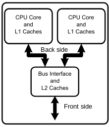
Within a multi-core processor, theback-side busis often internal, with front-side bus for external communication
Evolution
The front-side bus had the advantage of high flexibility and low cost. Simple symmetric multiprocessors place a number of CPUs on an FSB, though performance does not scale linearly due to the architecture's bandwidth bottleneck.
The front-side bus was used in all of Intel's Atom, Celeron, Pentium, Core 2, and Xeon processor models through about 2008. Originally, this bus was a central connecting point for all system devices and the CPU. The speed of a faster CPU is wasted if it cannot fetch instructions and data as fast as it can execute them. The CPU must wait for one or more clock cycles until the memory returns its value, or access other devices attached to the FSB if it becomes a bottleneck.
The front-side bus was criticized by AMD as being an old and slow technology that limits system performance.[8] More modern designs use point-to-point connections like AMD's HyperTransport and Intel's QuickPath Interconnect (QPI).[9] FSB's fastest transfer speed was 1.6 GT/s, which provided only 80% of the theoretical bandwidth of a 16-bit HyperTransport 3.0 link as implemented on AM3 Phenom II CPUs, only half of the bandwidth of a 6.4 GT/s QuickPath Interconnect link, and only 25% of the bandwidth of a 32-bit HyperTransport 3.1 link. In addition, in an FSB-based architecture, the memory must be accessed via the FSB. In HT- and QPI-based systems, the memory is accessed independently by means of a memory controller on the CPU itself, freeing bandwidth on the HyperTransport or QPI link for other uses.
intel
放弃了传统的FSB,使用了新的'Quick Path Interconnect',与AMD的HyperTransport相似。相比FSB,每一个处理器都可以有独立的QPI通道与其他处理器连接,处理器之间不用再共享FSB带宽,并绕路到北桥才能通讯。此外,QPI是双向传输[12]。