Use Clock and Register-Control Architectural Features
FPGAs provide device-wide clocks and register control signals that can improve performance.
Use Global Clock Network Resources
Altera FPGAs provide device-wide global clock routing resources and dedicated inputs. Use the FPGA’s low-skew, high fan-out dedicated routing where available.
FPGAs offer a number of low-skew global routing resources to distribute high fan-out signals to help withthe implementation of large designs with many clock domains.
Use Global Reset Resources
ASIC designs may use local resets to avoid long routing delays. Take advantage of the device-wide asynchronous reset pin available on most FPGAs to eliminate these problems. This reset signal provides low-skew routing across the device.
The following are three types of resets used in synchronous circuits:
• Synchronous Reset
• Asynchronous Reset
• Synchronized Asynchronous Reset—preferred when designing an FPGA circuit
Use Synchronous Resets
The synchronous reset ensures that the circuit is fully synchronous. You can easily time the circuit with the Quartus Prime TimeQuest analyzer.
Because clocks that are synchronous to each other launch and latch the reset signal, the data arrival and data required times are easily determined for proper slack analysis. The synchronous reset is easier to use with cycle-based simulators.
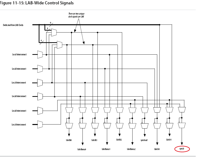
There are two methods by which a reset signal can reach a register; either by being gated in with the data input, or by using an LAB-wide control signal (synclr).

Consider two types of synchronous resets when you examine the timing analysis of synchronous resets—externally synchronized resets and internally synchronized resets.
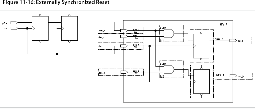


module sync_reset_ext (
input clock,
input reset_n,
input data_a,
input data_b,
output out_a,
output out_b
);
reg reg1, reg2;
assign out_a = reg1;
assign out_b = reg2;
always @ (posedge clock)
begin
if (!reset_n)
begin
reg1 <= 1’b0;
reg2 <= 1’b0;
end
else
begin
reg1 <= data_a;
reg2 <= data_b;
end
end
endmodule // sync_reset_ext
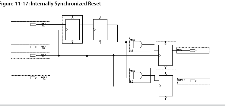
module sync_reset (
input clock,
input reset_n,
input data_a,
input data_b,
output out_a,
output out_b
);
reg reg1, reg2;
reg reg3, reg4;
assign out_a = reg1;
assign out_b = reg2;
assign rst_n = reg4;
always @ (posedge clock)
begin
if (!rst_n)
begin
reg1 <= 1’bo;
reg2 <= 1’b0;
end
else
begin
reg1 <= data_a;
reg2 <= data_b;
end
end
always @ (posedge clock)
begin
reg3 <= reset_n;
reg4 <= reg3;
end
endmodule // sync_reset
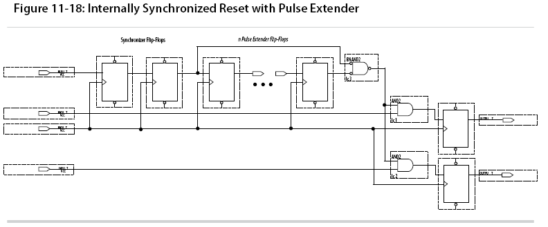
In some cases, you might want to increase the noise immunity further and reject any asynchronous input reset that is less than n periods wide to debounce an asynchronous input reset.
Using Asynchronous Resets
Asynchronous resets are the most common form of reset in circuit designs, as well as the easiest to implement.
However, when the reset is deasserted and does not pass the recovery (μtSU) or removal (μtH) time check (the TimeQuest analyzer recovery and removal analysis checks both times), the edge is said to have fallen into the metastability zone.
To avoid this, add a few follower registers after the register with the asynchronous reset and use the output of these registers in the
design.
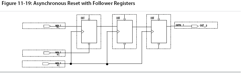
module async_reset (
input clock,
input reset_n,
input data_a,
output out_a,
);
reg reg1, reg2, reg3;
assign out_a = reg3;
always @ (posedge clock, negedge reset_n)
begin
if (!reset_n)
reg1 <= 1’b0;
else
reg1 <= data_a;
end
always @ (posedge clock)
begin
reg2 <= reg1;
reg3 <= reg2;
end
endmodule // async_reset
The asynchronous reset is susceptible to noise, and a noisy asynchronous reset can cause a spurious reset. You must ensure that the asynchronous reset is debounced and filtered. You can easily enter into a reset asynchronously, but releasing a reset asynchronously can lead to potential problems (also referred to as “reset removal”) with metastability, including the hazards of
unwanted situations with synchronous circuits involving feedback.
Use Synchronized Asynchronous Reset
To avoid potential problems associated with purely synchronous resets and purely asynchronous resets, you can use synchronized asynchronous resets. Synchronized asynchronous resets combine the advantages of synchronous and asynchronous resets.
This takes effect almost instantaneously, and ensures that no data path for speed is involved, and that the circuit is synchronous for timing analysis and is resistant to noise.
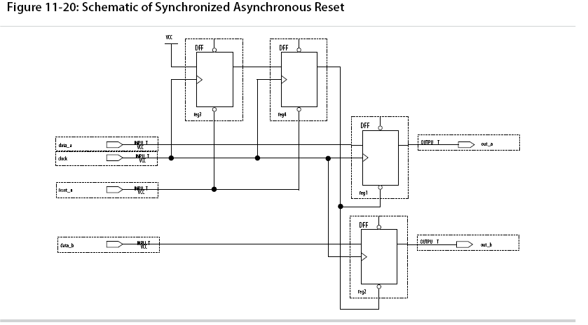
module sync_async_reset (
input clock,
input reset_n,
input data_a,
input data_b,
output out_a,
output out_b
);
reg reg1, reg2;
reg reg3, reg4;
assign out_a = reg1;
assign out_b = reg2;
assign rst_n = reg4;
always @ (posedge clock, negedge reset_n)
begin
if (!reset_n)
begin
reg3 <= 1’b0;
reg4 <= 1’b0;
end
else
begin
reg3 <= 1’b1;
reg4 <= reg3;
end
end
always @ (posedge clock, negedge rst_n)
begin
if (!rst_n)
begin
reg1 <= 1’b0;
reg2 <= 1;b0;
end
else
begin
reg1 <= data_a;
reg2 <= data_b;
end
end
endmodule // sync_async_reset
To minimize the metastability effect between the two synchronization registers, and to increase
the MTBF, the registers should be located as close as possible in the device to minimize routing delay. If possible, locate the registers in the same logic array block (LAB).
Avoid Asynchronous Register Control Signals
Avoid using an asynchronous load signal if the design target device architecture does not include registers with dedicated circuitry for asynchronous loads. Also, avoid using both asynchronous clear and preset if the architecture provides only one of these control signals.
When the target device does not directly support the signals, the synthesis or placement and routing software must use combinational logic to implement the same functionality. In addition, if you use signals in a priority other than the inherent priority in the device architecture, combinational logic may be required to implement the necessary control signals. Combinational logic is less efficient and can cause glitches and other problems; it is best to avoid these implementations.
Implementing Embedded RAM
Altera’s dedicated memory architecture offers many advanced features that you can enable with Altera provided IP cores. Use synchronous memory blocks for your design, so that the blocks can be mapped directly into the device dedicated memory blocks.
In many synthesis tools, you can specify that the read-during-write behavior is not important to your design; if, for example, you never read and write from the same address in the same clock cycle. For
Quartus Prime integrated synthesis, add the synthesis attribute ramstyle=”no_rw_check” to allow the software to choose the read-during-write behavior of a RAM, rather than using the read-during-write
behavior specified in your HDL code. Using this type of attribute prevents the synthesis tool from using extra logic to implement the memory block and, in some cases, can allow memory inference when it
would otherwise be impossible.