Optimizing Clocking Schemes
Avoid using internally generated clocks (other than PLLs) wherever possible because they can cause functional and timing problems in the design.
Use clock setting assignments on any derived or internal clocks to specify their relationship to the base clock.
Use global device-wide, low-skew dedicated routing for all internally-generated clocks, instead of
routing clocks on regular routing lines.
Avoid data transfers between different clocks wherever possible. If you require a data transfer between different clocks, use FIFO circuitry.
You can use the clock uncertainty features in the Quartus Prime software to compensate for the variable delays between clock domains. Consider setting a clock setup uncertainty and clock hold uncertainty value of 10% to 15% of the clock delay.
Register Combinational Logic Outputs
If you use the output from combinational logic as a clock signal or as an asynchronous reset signal, you can expect to see glitches in your design. In a synchronous design, glitches on data inputs of registers are normal events that have no consequences. However, a glitch or a spike on the clock input (or an asynchronous input) to a register can have significant consequences.
To avoid these problems, you should always register the output of combinational logic before you use it as a clock signal.

Avoid Asyncrhonous Clock Division
Using dedicated PLL circuitry can help you to avoid many of the problems that can be introduced by asynchronous clock division logic.
When you must use logic to divide a master clock, always use synchronous counters or state machines. Additionally, create your design so that registers always directly generate divided clock signals, and route the clock on global clock resources. To avoid glitches, do not decode the outputs of a counter or a state machine to generate clock signals.
Avoid Ripple Counters
Ripple counters use cascaded registers, in which the output pin of one register feeds the clock pin of the register in the next stage. This cascading can cause problems because the counter creates a ripple clock at each stage. These ripple clocks must be handled properly during timing analysis, which can be difficult and may require you to make complicated timing assignments in your synthesis and placement and routing tools.
Use Multiplexed Clocks
Use clock multiplexing to operate the same logic function with different clock sources. In these designs, multiplexing selects a clock source.
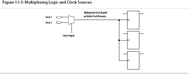
Adding multiplexing logic to the clock signal can create the problems addressed in the previous sections, but requirements for multiplexed clocks vary widely, depending on the application. Clock multiplexing is acceptable when the clock signal uses global clock routing resources and if the following criteria are met:
• The clock multiplexing logic does not change after initial configuration
• The design uses multiplexing logic to select a clock for testing purposes
• Registers are always reset when the clock switches
• A temporarily incorrect response following clock switching has no negative consequences
Use Gated Clocks
Gated clocks turn a clock signal on and off using an enable signal that controls gating circuitry.
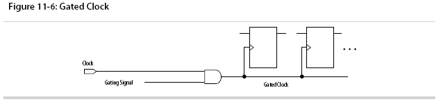
You can use gated clocks to reduce power consumption in some device architectures by effectively shutting down portions of a digital circuit when they are not in use. When a clock is gated, both the clock network and the registers driven by it stop toggling, thereby eliminating their contributions to power consumption. However, gated clocks are not part of a synchronous scheme and therefore can significantly increase the effort required for design implementation and verification. Gated clocks contribute to clock skew and make device migration difficult. These clocks are also sensitive to glitches, which can cause design failure.
Use dedicated hardware to perform clock gating rather than an AND or OR gate.
From a functional point of view, you can shut down a clock domain in a purely synchronous manner using a synchronous clock enable signal.
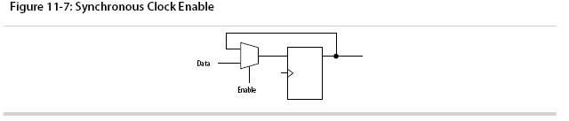
Use Synchronous Clock Enables
To turn off a clock domain in a synchronous manner, use a synchronous clock enable signal. FPGAs efficiently support clock enable signals because there is a dedicated clock enable signal available on all device registers.
This scheme does not reduce power consumption as much as gating the clock at the source because the clock network keeps toggling, and performs the same function as a gated clock by disabling a set of registers. Insert a multiplexer in front of the data input of every register to either load new data, or copy the output of the register.
Recommended Clock-Gating Methods
Use gated clocks only when your target application requires power reduction and when gated clocks are able to provide the required reduction in your device architecture.
If you must use clocks gated by logic, implement these clocks using the robust clock-gating technique and ensure that the gated clock signal uses dedicated global clock routing.
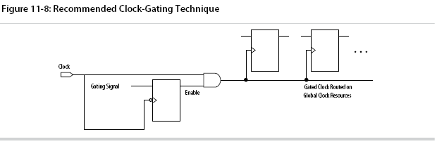
The register that generates the enable signal is triggered on the inactive edge of the clock to be gated. Use the falling edge when gating a clock that is active on the rising edge. Using this technique, only one input of the gate that turns the clock on and off changes at a time. This prevents glitches or spikes on the output.