本文写的非常好,但是翻译的质量不是很好,因此本文基于翻译做了修改。
转自http://www.oschina.net/translate/what-every-programmer-should-know-about-memory-part1
| [ Editor's introduction: Ulrich Drepper recently approached us asking if we would be interested in publishing a lengthy document he had written on how memory and software interact. We did not have to look at the text for long to realize that it would be of interest to many LWN readers. Memory usage is often the determining factor in how software performs, but good information on how to avoid memory bottlenecks is hard to find. This series of articles should change that situation.
The original document prints out at over 100 pages. We will be splitting it into about seven segments, each run 1-2 weeks after its predecessor. Once the entire series is out, Ulrich will be releasing the full text. Reformatting the text from the original LaTeX has been a bit of a challenge, but the results, hopefully, will be good. For ease of online reading, Ulrich's footnotes have been placed {inline in the text}. Hyperlinked cross-references (and [bibliography references]) will not be possible until the full series is published. Many thanks to Ulrich for allowing LWN to publish this material; we hope that it will lead to more memory-efficient software across our systems in the near future.] |
译者信息
[编辑的话: Ulrich Drepper最近问我们,是不是有兴趣发表一篇他写的内存方面的长文。我们不用看太多就已经知道,LWN的读者们会喜欢这篇文章的。内存的使用常常是软件性能的决定性因子,而如何避免内存瓶颈的好文章却不好找。这篇文章应该会有所帮助。 他的原文很长,超过100页。我们把它分成了7篇,每隔一到两周发表一篇。7篇发完后,Ulrich会把全文发出来。 对原文重新格式化是个很有挑战性的工作,但愿结果会不错吧。为了便于网上阅读,我们把Ulrich的脚注{放在了文章里},而互相引用的超链接(和[参考书目])要等到全文出来才能提供。 非常感谢Ultich,感谢他让LWN发表这篇文章,期待大家在不久的将来都能写出内存优化很棒的软件。] |
||||||||||||||||||||||||||||||||||||||||||||||||||||||||||||
1 IntroductionIn the early days computers were much simpler. The various components of a system, such as the CPU, memory, mass storage, and network interfaces, were developed together and, as a result, were quite balanced in their performance. For example, the memory and network interfaces were not (much) faster than the CPU at providing data. This situation changed once the basic structure of computers stabilized and hardware developers concentrated on optimizing individual subsystems. Suddenly the performance of some components of the computer fell significantly behind and bottlenecks developed. This was especially true for mass storage and memory subsystems which, for cost reasons, improved more slowly relative to other components. |
译者信息
1 简介早期计算机比现在更为简单。系统的各种组件例如CPU,内存,大容量存储器和网口,由于被共同开发因而有非常均衡的表现。例如,内存和网口并不比CPU在提供数据的时候更(特别的)快。 随着计算机稳定的基本结构,硬件开发人员开始致力于优化单个子系统,情况开始发生变化。于是电脑一些组件的性能大大的落后因而成为了瓶颈。由于成本原因,大容量存储器和内存子系统相对于其他组件来说改善得更为缓慢。 |
||||||||||||||||||||||||||||||||||||||||||||||||||||||||||||
|
The slowness of mass storage has mostly been dealt with using software techniques: operating systems keep most often used (and most likely to be used) data in main memory, which can be accessed at a rate orders of magnitude faster than the hard disk. Cache storage was added to the storage devices themselves, which requires no changes in the operating system to increase performance. {Changes are needed, however, to guarantee data integrity when using storage device caches.} For the purposes of this paper, we will not go into more details of software optimizations for the mass storage access. Unlike storage subsystems, removing the main memory as a bottleneck has proven much more difficult and almost all solutions require changes to the hardware. Today these changes mainly come in the following forms:
|
译者信息
大多情况下,采用软件技术解决大容量存储的慢的问题。如:操作系统将常用(且最有可能被用)的数据放在主存中,因为它比内存快上好几个数量级。或者将缓存加入存储设备中,这样就可以在不修改操作系统的前提下提升性能。{然而,为了在使用缓存时保证数据的完整性,仍然要作出一些修改。}这些内容不在本文的谈论范围之内,就不作赘述了。 与存储子系统不同,消除内存瓶颈非常困难,而且几乎每种方案都需要对硬件作出修改。目前,这些变更主要有以下这些方式:
|
||||||||||||||||||||||||||||||||||||||||||||||||||||||||||||
| For the most part, this document will deal with CPU caches and some effects of memory controller design. In the process of exploring these topics, we will explore DMA and bring it into the larger picture. However, we will start with an overview of the design for today's commodity hardware. This is a prerequisite to understanding the problems and the limitations of efficiently using memory subsystems. We will also learn about, in some detail, the different types of RAM and illustrate why these differences still exist.
This document is in no way all inclusive and final. It is limited to commodity hardware and further limited to a subset of that hardware. Also, many topics will be discussed in just enough detail for the goals of this paper. For such topics, readers are recommended to find more detailed documentation. |
译者信息
本文主要关心的是CPU缓存和内存控制器的设计的一些效果。在讨论这些主题的过程中,我们还会研究DMA。不过,我们首先会从当今商用硬件的设计谈起。这有助于我们理解目前在使用内存子系统时可能遇到的问题和限制。我们还会详细介绍RAM的分类,说明为什么会存在这么多不同类型的内存。 本文不会包括所有内容,也不会包括最终性质的内容。我们的讨论范围仅止于商用硬件,而且只限于其中的一小部分。另外,本文中的许多论题,我们只会点到为止,以达到本文目标为标准。对于这些论题,大家可以阅读其它文档,获得更详细的说明。 |
||||||||||||||||||||||||||||||||||||||||||||||||||||||||||||
|
When it comes to operating-system-specific details and solutions, the text exclusively describes Linux. At no time will it contain any information about other OSes. The author has no interest in discussing the implications for other OSes. If the reader thinks s/he has to use a different OS they have to go to their vendors and demand they write documents similar to this one. One last comment before the start. The text contains a number of occurrences of the term “usually” and other, similar qualifiers. The technology discussed here exists in many, many variations in the real world and this paper only addresses the most common, mainstream versions. It is rare that absolute statements can be made about this technology, thus the qualifiers. |
译者信息
当本文提到操作系统特定的细节和解决方案时,针对的都是Linux。无论何时都不会包含别的操作系统的任何信息,作者无意讨论其他操作系统的情况。如果读者认为他/她不得不使用别的操作系统,那么必须去要求供应商提供其操作系统类似于本文的文档。 在开始之前最后的一点说明,本文包含大量出现的术语“经常”和别的类似的限定词。这里讨论的技术在现实中存在于很多不同的实现,所以本文只阐述使用得最广泛最主流的版本。在阐述中很少有地方能用到绝对的限定词。 |
||||||||||||||||||||||||||||||||||||||||||||||||||||||||||||
1.1 Document StructureThis document is mostly for software developers. It does not go into enough technical details of the hardware to be useful for hardware-oriented readers. But before we can go into the practical information for developers a lot of groundwork must be laid. To that end, the second section describes random-access memory (RAM) in technical detail. This section's content is nice to know but not absolutely critical to be able to understand the later sections. Appropriate back references to the section are added in places where the content is required so that the anxious reader could skip most of this section at first. The third section goes into a lot of details of CPU cache behavior. Graphs have been used to keep the text from being as dry as it would otherwise be. This content is essential for an understanding of the rest of the document. Section 4 describes briefly how virtual memory is implemented. This is also required groundwork for the rest. |
译者信息
1.1文档结构这个文档主要视为软件开发者而写的。本文不会涉及太多硬件细节,所以喜欢硬件的读者也许不会觉得有用。但是在我们讨论一些有用的细节之前,我们先要描述足够多的背景。 在这个基础上,本文的第二部分将描述RAM(随机寄存器)。懂得这个部分的内容很好,但是此部分的内容并不是懂得其后内容必须部分。我们会在之后引用不少之前的部分,所以心急的读者可以先跳过这本分。 第三部分会谈到不少关于CPU缓存行为模式的内容。我们会列出一些图标,这样你们不至于觉得太枯燥。第三部分对于理解整个文章非常重要。第四部分将简短的描述虚拟内存是怎么被实现的。这也是理解其他部分的背景知识。 |
||||||||||||||||||||||||||||||||||||||||||||||||||||||||||||
|
Section 5 goes into a lot of detail about Non Uniform Memory Access (NUMA) systems. Section 6 is the central section of this paper. It brings together all the previous sections' information and gives programmers advice on how to write code which performs well in the various situations. The very impatient reader could start with this section and, if necessary, go back to the earlier sections to freshen up the knowledge of the underlying technology. Section 7 introduces tools which can help the programmer do a better job. Even with a complete understanding of the technology it is far from obvious where in a non-trivial software project the problems are. Some tools are necessary. In section 8 we finally give an outlook of technology which can be expected in the near future or which might just simply be good to have. |
译者信息
第五部分会提到许多关于Non Uniform Memory Access (NUMA)系统。 第六部分是本文的中心部分。在这个部分里面,我们将回顾其他许多部分中的信息,并且我们将给阅读本文的程序员许多在各种情况下的编程建议。如果你真的很心急,那么你可以直接阅读第六部分,并且我们建议你在必要的时候回到之前的章节回顾一下必要的背景知识。 本文的第七部分将介绍一些能够帮助程序员更好的完成任务的工具。即便在彻底理解了某一项技术的情况下,距离彻底理解在非测试环境下的程序还是很遥远的。我们需要借助一些工具。 第八部分,我们将展望一些在未来我们可能认为好用的科技。 |
||||||||||||||||||||||||||||||||||||||||||||||||||||||||||||
1.2 Reporting ProblemsThe author intends to update this document for some time. This includes updates made necessary by advances in technology but also to correct mistakes. Readers willing to report problems are encouraged to send email. 1.3 ThanksI would like to thank Johnray Fuller and especially Jonathan Corbet for taking on part of the daunting task of transforming the author's form of English into something more traditional. Markus Armbruster provided a lot of valuable input on problems and omissions in the text. 1.4 About this DocumentThe title of this paper is an homage to David Goldberg's classic paper “What Every Computer Scientist Should Know About Floating-Point Arithmetic” [goldberg]. Goldberg's paper is still not widely known, although it should be a prerequisite for anybody daring to touch a keyboard for serious programming. |
译者信息
1.2 反馈问题 作者会不定期更新本文档。这些更新既包括伴随技术进步而来的更新也包含更改错误。非常欢迎有志于反馈问题的读者发送电子邮件。 1.3 致谢 我首先需要感谢Johnray Fuller尤其是Jonathan Corbet,感谢他们将作者的英语转化成为更为规范的形式。Markus Armbruster提供大量本文中对于问题和缩写有价值的建议。 1.4 关于本文 本文题目对David Goldberg的经典文献《What Every Computer Scientist Should Know About Floating-Point Arithmetic》[goldberg]表示致敬。Goldberg的论文虽然不普及,但是对于任何有志于严格编程的人都会是一个先决条件。 |
||||||||||||||||||||||||||||||||||||||||||||||||||||||||||||
2 Commodity Hardware TodayUnderstanding commodity hardware is important because specialized hardware is in retreat. Scaling these days is most often achieved horizontally instead of vertically, meaning today it is more cost-effective to use many smaller, connected commodity computers instead of a few really large and exceptionally fast (and expensive) systems. This is the case because fast and inexpensive network hardware is widely available. There are still situations where the large specialized systems have their place and these systems still provide a business opportunity, but the overall market is dwarfed by the commodity hardware market. Red Hat, as of 2007, expects that for future products, the “standard building blocks” for most data centers will be a computer with up to four sockets, each filled with a quad core CPU that, in the case of Intel CPUs, will be hyper-threaded. {Hyper-threading enables a single processor core to be used for two or more concurrent executions with just a little extra hardware.} This means the standard system in the data center will have up to 64 virtual processors. Bigger machines will be supported, but the quad socket, quad CPU core case is currently thought to be the sweet spot and most optimizations are targeted for such machines. |
译者信息
2 商用硬件现状鉴于目前专用硬件正在逐渐淡出,理解商用硬件的现状变得十分重要。现如今,人们更多的采用水平扩展,也就是说,用大量小型、互联的商用计算机代替巨大、超快(但超贵)的系统。原因在于,快速而廉价的网络硬件已经崛起。那些大型的专用系统仍然有一席之地,但已被商用硬件后来居上。2007年,Red Hat认为,未来构成数据中心的“积木”将会是拥有最多4个插槽的计算机,每个插槽插入一个四核CPU,这些CPU都是超线程的。{超线程使单个处理器核心能同时处理两个以上的任务,只需加入一点点额外硬件}。也就是说,这些数据中心中的标准系统拥有最多64个虚拟处理器。当然可以支持更大的系统,但人们认为4插槽、4核CPU是最佳配置,绝大多数的优化都针对这样的配置。 |
||||||||||||||||||||||||||||||||||||||||||||||||||||||||||||
|
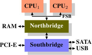
Large differences exist in the structure of commodity computers. That said, we will cover more than 90% of such hardware by concentrating on the most important differences. Note that these technical details tend to change rapidly, so the reader is advised to take the date of this writing into account. Over the years the personal computers and smaller servers standardized on a chipset with two parts: the Northbridge and Southbridge. Figure 2.1 shows this structure.
All CPUs (two in the previous example, but there can be more) are connected via a common bus (the Front Side Bus, FSB) to the Northbridge. The Northbridge contains, among other things, the memory controller, and its implementation determines the type of RAM chips used for the computer. Different types of RAM, such as DRAM, Rambus, and SDRAM, require different memory controllers. |
译者信息
在不同商用计算机之间,也存在着巨大的差异。不过,我们关注在主要的差异上,可以涵盖到超过90%以上的硬件。需要注意的是,这些技术上的细节往往日新月异,变化极快,因此大家在阅读的时候也需要注意本文的写作时间。 这么多年来,个人计算机和小型服务器被标准化到了一个芯片组上,它由两部分组成: 北桥和南桥,见图2.1。
CPU通过一条通用总线(前端总线,FSB)连接到北桥。北桥主要包括内存控制器和其它一些组件,内存控制器决定了RAM芯片的类型。不同的类型,包括DRAM、Rambus和SDRAM等等,要求不同的内存控制器。 |
||||||||||||||||||||||||||||||||||||||||||||||||||||||||||||
|
To reach all other system devices, the Northbridge must communicate with the Southbridge. The Southbridge, often referred to as the I/O bridge, handles communication with devices through a variety of different buses. Today the PCI, PCI Express, SATA, and USB buses are of most importance, but PATA, IEEE 1394, serial, and parallel ports are also supported by the Southbridge. Older systems had AGP slots which were attached to the Northbridge. This was done for performance reasons related to insufficiently fast connections between the Northbridge and Southbridge. However, today the PCI-E slots are all connected to the Southbridge. Such a system structure has a number of noteworthy consequences:
|
译者信息
为了连通其它系统设备,北桥需要与南桥通信。南桥又叫I/O桥,通过多条不同总线与设备们通信。目前,比较重要的总线有PCI、PCI Express、SATA和USB总线,除此以外,南桥还支持PATA、IEEE 1394、串行口和并行口等。比较老的系统上有连接北桥的AGP槽。那是由于南北桥间缺乏高速连接而采取的措施。现在的PCI-E都是直接连到南桥的。 这种结构有一些需要注意的地方:
|
||||||||||||||||||||||||||||||||||||||||||||||||||||||||||||
| A couple of bottlenecks are immediately apparent in this design. One such bottleneck involves access to RAM for devices. In the earliest days of the PC, all communication with devices on either bridge had to pass through the CPU, negatively impacting overall system performance. To work around this problem some devices became capable of direct memory access (DMA). DMA allows devices, with the help of the Northbridge, to store and receive data in RAM directly without the intervention of the CPU (and its inherent performance cost). Today all high-performance devices attached to any of the buses can utilize DMA. While this greatly reduces the workload on the CPU, it also creates contention for the bandwidth of the Northbridge as DMA requests compete with RAM access from the CPUs. This problem, therefore, must to be taken into account. |
译者信息 在上面这种设计中,瓶颈马上出现了。第一个瓶颈与设备对RAM的访问有关。早期,所有设备之间的通信都需要经过CPU,结果严重影响了整个系统的性能。为了解决这个问题,有些设备加入了直接内存访问(DMA)的能力。DMA允许设备在北桥的帮助下,无需CPU的干涉,直接读写RAM。到了今天,所有高性能的设备都可以使用DMA。虽然DMA大大降低了CPU的负担,却占用了北桥的带宽,与CPU形成了争用。 |
||||||||||||||||||||||||||||||||||||||||||||||||||||||||||||
|
A second bottleneck involves the bus from the Northbridge to the RAM. The exact details of the bus depend on the memory types deployed. On older systems there is only one bus to all the RAM chips, so parallel access is not possible. Recent RAM types require two separate buses (or channels as they are called for DDR2, see Figure 2.8) which doubles the available bandwidth. The Northbridge interleaves memory access across the channels. More recent memory technologies (FB-DRAM, for instance) add more channels. With limited bandwidth available, it is important to schedule memory access in ways that minimize delays. As we will see, processors are much faster and must wait to access memory, despite the use of CPU caches. If multiple hyper-threads, cores, or processors access memory at the same time, the wait times for memory access are even longer. This is also true for DMA operations. |
译者信息
第二个瓶颈来自北桥与RAM间的总线。总线的具体情况与内存的类型有关。在早期的系统上,只有一条总线,因此不能实现并行访问。近期的RAM需要两条独立总线(或者说通道,DDR2就是这么叫的,见图2.8),可以实现带宽加倍。北桥将内存访问交错地分配到两个通道上。更新的内存技术(如FB-DRAM)甚至加入了更多的通道。 由于带宽有限,我们需要以一种使延迟最小化的方式来对内存访问进行调度。我们将会看到,处理器的速度比内存要快得多,需要等待内存。如果有多个超线程核心或CPU同时访问内存,等待时间则会更长。对于DMA也是同样。 |
||||||||||||||||||||||||||||||||||||||||||||||||||||||||||||
|
There is more to accessing memory than concurrency, however. Access patterns themselves also greatly influence the performance of the memory subsystem, especially with multiple memory channels. Refer to Section 2.2 for more details of RAM access patterns. On some more expensive systems, the Northbridge does not actually contain the memory controller. Instead the Northbridge can be connected to a number of external memory controllers (in the following example, four of them).
|
译者信息
除了并发以外,访问模式也会极大地影响内存子系统、特别是多通道内存子系统的性能。关于访问模式,可参见2.2节。 在一些比较昂贵的系统上,北桥自己不含内存控制器,而是连接到外部的多个内存控制器上(在下例中,共有4个)。
|
||||||||||||||||||||||||||||||||||||||||||||||||||||||||||||
| The advantage of this architecture is that more than one memory bus exists and therefore total bandwidth increases. This design also supports more memory. Concurrent memory access patterns reduce delays by simultaneously accessing different memory banks. This is especially true when multiple processors are directly connected to the Northbridge, as in Figure 2.2. For such a design, the primary limitation is the internal bandwidth of the Northbridge, which is phenomenal for this architecture (from Intel). { For completeness it should be mentioned that such a memory controller arrangement can be used for other purposes such as “memory RAID” which is useful in combination with hotplug memory.} |
译者信息 这种架构的好处在于,多条内存总线的存在,使得总带宽也随之增加了。而且也可以支持更多的内存。通过同时访问不同内存区,还可以降低延时。对于像图2.2中这种多处理器直连北桥的设计来说,尤其有效。而这种架构的局限在于北桥的内部带宽,非常巨大(来自Intel)。{出于完整性的考虑,还需要补充一下,这样的内存控制器布局还可以用于其它用途,比如说「内存RAID」,它可以与热插拔技术一起使用。} |
||||||||||||||||||||||||||||||||||||||||||||||||||||||||||||
|
Using multiple external memory controllers is not the only way to increase memory bandwidth. One other increasingly popular way is to integrate memory controllers into the CPUs and attach memory to each CPU. This architecture is made popular by SMP systems based on AMD's Opteron processor. Figure 2.3 shows such a system. Intel will have support for the Common System Interface (CSI) starting with the Nehalem processors; this is basically the same approach: an integrated memory controller with the possibility of local memory for each processor.
With an architecture like this there are as many memory banks available as there are processors. On a quad-CPU machine the memory bandwidth is quadrupled without the need for a complicated Northbridge with enormous bandwidth. Having a memory controller integrated into the CPU has some additional advantages; we will not dig deeper into this technology here. |
译者信息
使用外部内存控制器并不是唯一的办法,另一个最近比较流行的方法是将控制器集成到CPU内部,将内存直连到每个CPU。这种架构的走红归功于基于AMD Opteron处理器的SMP系统。图2.3展示了这种架构。Intel则会从Nehalem处理器开始支持通用系统接口(CSI),基本上也是类似的思路——集成内存控制器,为每个处理器提供本地内存。
通过采用这样的架构,系统里有几个处理器,就可以有几个内存库(memory bank)。比如,在4 CPU的计算机上,不需要一个拥有巨大带宽的复杂北桥,就可以实现4倍的内存带宽。另外,将内存控制器集成到CPU内部还有其它一些优点,这里就不赘述了。 |
||||||||||||||||||||||||||||||||||||||||||||||||||||||||||||
|
There are disadvantages to this architecture, too. First of all, because the machine still has to make all the memory of the system accessible to all processors, the memory is not uniform anymore (hence the name NUMA - Non-Uniform Memory Architecture - for such an architecture). Local memory (memory attached to a processor) can be accessed with the usual speed. The situation is different when memory attached to another processor is accessed. In this case the interconnects between the processors have to be used. To access memory attached to CPU2 from CPU1 requires communication across one interconnect. When the same CPU accesses memory attached to CPU4 two interconnects have to be crossed. Each such communication has an associated cost. We talk about “NUMA factors” when we describe the extra time needed to access remote memory. The example architecture in Figure 2.3 has two levels for each CPU: immediately adjacent CPUs and one CPU which is two interconnects away. With more complicated machines the number of levels can grow significantly. There are also machine architectures (for instance IBM's x445 and SGI's Altix series) where there is more than one type of connection. CPUs are organized into nodes; within a node the time to access the memory might be uniform or have only small NUMA factors. The connection between nodes can be very expensive, though, and the NUMA factor can be quite high. |
译者信息
同样也有缺点。首先,系统仍然要让所有内存能被所有处理器所访问,导致内存不再是统一的资源(NUMA即得名于此)。处理器能以正常的速度访问本地内存(连接到该处理器的内存)。但它访问其它处理器的内存时,却需要使用处理器之间的互联通道。比如说,CPU 1如果要访问CPU 2的内存,则需要使用它们之间的互联通道。如果它需要访问CPU 4的内存,那么需要跨越两条互联通道。 使用互联通道是有代价的。在讨论访问远端内存的代价时,我们用「NUMA因子」这个词。在图2.3中,每个CPU有两个层级: 相邻的CPU,以及两个互联通道外的CPU。在更加复杂的系统中,层级也更多。甚至有些机器有不止一种连接,比如说IBM的x445和SGI的Altix系列。CPU被归入节点,节点内的内存访问时间是一致的,或者只有很小的NUMA因子。而在节点之间的连接代价很大,而且有巨大的NUMA因子。 |
||||||||||||||||||||||||||||||||||||||||||||||||||||||||||||
|
Commodity NUMA machines exist today and will likely play an even greater role in the future. It is expected that, from late 2008 on, every SMP machine will use NUMA. The costs associated with NUMA make it important to recognize when a program is running on a NUMA machine. In Section 5 we will discuss more machine architectures and some technologies the Linux kernel provides for these programs. Beyond the technical details described in the remainder of this section, there are several additional factors which influence the performance of RAM. They are not controllable by software, which is why they are not covered in this section. The interested reader can learn about some of these factors in Section 2.1. They are really only needed to get a more complete picture of RAM technology and possibly to make better decisions when purchasing computers. The following two sections discuss hardware details at the gate level and the access protocol between the memory controller and the DRAM chips. Programmers will likely find this information enlightening since these details explain why RAM access works the way it does. It is optional knowledge, though, and the reader anxious to get to topics with more immediate relevance for everyday life can jump ahead to Section 2.2.5. |
译者信息
目前,已经有商用的NUMA计算机,而且它们在未来应该会扮演更加重要的角色。人们预计,从2008年底开始,每台SMP机器都会使用NUMA。每个在NUMA上运行的程序都应该认识到NUMA的代价。在第5节中,我们将讨论更多的架构,以及Linux内核为这些程序提供的一些技术。 除了本节中所介绍的技术之外,还有其它一些影响RAM性能的因素。它们无法被软件所左右,所以没有放在这里。如果大家有兴趣,可以在第2.1节中看一下。介绍这些技术,仅仅是因为它们能让我们绘制的RAM技术全图更为完整,或者是可能在大家购买计算机时能够提供一些帮助。 以下的两节主要介绍一些入门级的硬件知识,同时讨论内存控制器与DRAM芯片间的访问协议。这些知识解释了内存访问的原理,程序员可能会得到一些启发。不过,这部分并不是必读的,心急的读者可以直接跳到第2.2.5节。 |
||||||||||||||||||||||||||||||||||||||||||||||||||||||||||||
2.1 RAM TypesThere have been many types of RAM over the years and each type varies, sometimes significantly, from the other. The older types are today really only interesting to the historians. We will not explore the details of those. Instead we will concentrate on modern RAM types; we will only scrape the surface, exploring some details which are visible to the kernel or application developer through their performance characteristics. The first interesting details are centered around the question why there are different types of RAM in the same machine. More specifically, why there are both static RAM (SRAM {In other contexts SRAM might mean “synchronous RAM”.}) and dynamic RAM (DRAM). The former is much faster and provides the same functionality. Why is not all RAM in a machine SRAM? The answer is, as one might expect, cost. SRAM is much more expensive to produce and to use than DRAM. Both these cost factors are important, the second one increasing in importance more and more. To understand these difference we look at the implementation of a bit of storage for both SRAM and DRAM. In the remainder of this section we will discuss some low-level details of the implementation of RAM. We will keep the level of detail as low as possible. To that end, we will discuss the signals at a “logic level” and not at a level a hardware designer would have to use. That level of detail is unnecessary for our purpose here. |
译者信息
2.1 RAM类型这些年来,出现了许多不同类型的RAM,各有差异,有些甚至有非常巨大的不同。那些很古老的类型已经乏人问津,我们就不仔细研究了。我们主要专注于几类现代RAM,剖开它们的表面,研究一下内核和应用开发人员们可以看到的一些细节。 第一个有趣的细节是,为什么在同一台机器中有不同的RAM?或者说得更详细一点,为什么既有静态RAM(SRAM {SRAM还可以表示「同步内存」。}),又有动态RAM(DRAM)。功能相同,前者更快。那么,为什么不全部使用SRAM?答案是,代价。无论在生产还是在使用上,SRAM都比DRAM要贵得多。生产和使用,这两个代价因子都很重要,后者则是越来越重要。为了理解这一点,我们分别看一下SRAM和DRAM一个位的存储的实现过程。 在本节的余下部分,我们将讨论RAM实现的底层细节。我们将尽量控制细节的层面,比如,在「逻辑的层面」讨论信号,而不是硬件设计师那种层面,因为那毫无必要。 |
||||||||||||||||||||||||||||||||||||||||||||||||||||||||||||
|
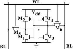
2.1.1 Static RAM
Figure 2.4 shows the structure of a 6 transistor SRAM cell. The core of this cell is formed by the four transistorsM1toM4which form two cross-coupled inverters. They have two stable states, representing 0 and 1 respectively. The state is stable as long as power onVddis available. If access to the state of the cell is needed the word access lineWLis raised. This makes the state of the cell immediately available for reading onBLandBL. If the cell state must be overwritten theBLandBLlines are first set to the desired values and thenWLis raised. Since the outside drivers are stronger than the four transistors (M1throughM4) this allows the old state to be overwritten. See [sramwiki] for a more detailed description of the way the cell works. For the following discussion it is important to note that
There are other, slower and less power-hungry, SRAM forms available, but those are not of interest here since we are looking at fast RAM. These slow variants are mainly interesting because they can be more easily used in a system than dynamic RAM because of their simpler interface. |
译者信息
2.1.1 静态RAM
图2.4展示了6晶体管SRAM的一个单元。核心是4个晶体管M1-M4,它们组成两个交叉耦合的反相器。它们有两个稳定的状态,分别代表0和1。只要保持Vdd有电,状态就是稳定的。 当需要访问单元的状态时,升起字访问线WL。BL和BL上就可以读取状态。如果需要覆盖状态,先将BL和BL设置为期望的值,然后升起WL。由于外部的驱动强于内部的4个晶体管,所以旧状态会被覆盖。 更多详情,可以参考[sramwiki]。为了下文的讨论,需要注意以下问题: 一个单元需要6个晶体管。也有采用4个晶体管的SRAM,但有缺陷。 维持状态需要恒定的电源。 升起WL后立即可以读取状态。信号与其它晶体管控制的信号一样,是直角的(快速在两个状态间变化)。 状态稳定,不需要刷新循环。 SRAM也有其它形式,不那么费电,但比较慢。由于我们需要的是快速RAM,因此不在关注范围内。这些较慢的SRAM的主要优点在于接口简单,比动态RAM更容易使用。 |
||||||||||||||||||||||||||||||||||||||||||||||||||||||||||||
|
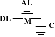
2.1.2 Dynamic RAM Dynamic RAM is, in its structure, much simpler than static RAM. Figure 2.5 shows the structure of a usual DRAM cell design. All it consists of is one transistor and one capacitor. This huge difference in complexity of course means that it functions very differently than static RAM.
A dynamic RAM cell keeps its state in the capacitorC. The transistorMis used to guard the access to the state. To read the state of the cell the access lineALis raised; this either causes a current to flow on the data lineDLor not, depending on the charge in the capacitor. To write to the cell the data lineDLis appropriately set and thenALis raised for a time long enough to charge or drain the capacitor. There are a number of complications with the design of dynamic RAM. The use of a capacitor means that reading the cell discharges the capacitor. The procedure cannot be repeated indefinitely, the capacitor must be recharged at some point. Even worse, to accommodate the huge number of cells (chips with 109 or more cells are now common) the capacity to the capacitor must be low (in the femto-farad range or lower). A fully charged capacitor holds a few 10's of thousands of electrons. Even though the resistance of the capacitor is high (a couple of tera-ohms) it only takes a short time for the capacity to dissipate. This problem is called “leakage”. |
译者信息
2.1.2 动态RAM动态RAM比静态RAM要简单得多。图2.5展示了一种普通DRAM的结构。它只含有一个晶体管和一个电容器。显然,这种复杂性上的巨大差异意味着功能上的迥异。
动态RAM的状态是保持在电容器C中。晶体管M用来控制访问。如果要读取状态,升起访问线AL,这时,可能会有电流流到数据线DL上,也可能没有,取决于电容器是否有电。如果要写入状态,先设置DL,然后升起AL一段时间,直到电容器充电或放电完毕。 动态RAM的设计有几个复杂的地方。由于读取状态时需要对电容器放电,所以这一过程不能无限重复,不得不在某个点上对它重新充电。 更糟糕的是,为了容纳大量单元(现在一般在单个芯片上容纳10的9次方以上的RAM单元),电容器的容量必须很小(0.000000000000001法拉以下)。这样,完整充电后大约持有几万个电子。即使电容器的电阻很大(若干兆欧姆),仍然只需很短的时间就会耗光电荷,称为「泄漏」。 |
||||||||||||||||||||||||||||||||||||||||||||||||||||||||||||
|
This leakage is why a DRAM cell must be constantly refreshed. For most DRAM chips these days this refresh must happen every 64ms. During the refresh cycle no access to the memory is possible. For some workloads this overhead might stall up to 50% of the memory accesses (see [highperfdram]). A second problem resulting from the tiny charge is that the information read from the cell is not directly usable. The data line must be connected to a sense amplifier which can distinguish between a stored 0 or 1 over the whole range of charges which still have to count as 1. A third problem is that charging and draining a capacitor is not instantaneous. The signals received by the sense amplifier are not rectangular, so a conservative estimate as to when the output of the cell is usable has to be used. The formulas for charging and discharging a capacitor are |
译者信息
这种泄露就是现在的大部分DRAM芯片每隔64ms就必须进行一次刷新的原因。在刷新期间,对于该芯片的访问是不可能的,这甚至会造成半数任务的延宕。(相关内容请察看【highperfdram】一章) 这个问题的另一个后果就是无法直接读取芯片单元中的信息,而必须通过信号放大器将0和1两种信号间的电势差增大。 最后一个问题在于电容器的冲放电是需要时间的,这就导致了信号放大器读取的信号并不是典型的矩形信号。所以当放大器输出信号的时候就需要一个小小的延宕,相关公式如下 |
||||||||||||||||||||||||||||||||||||||||||||||||||||||||||||
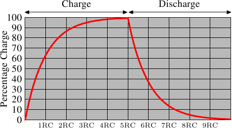
This means it takes some time (determined by the capacity C and resistance R) for the capacitor to be charged and discharged. It also means that the current which can be detected by the sense amplifiers is not immediately available. Figure 2.6 shows the charge and discharge curves. The X—axis is measured in units of RC (resistance multiplied by capacitance) which is a unit of time.
Unlike the static RAM case where the output is immediately available when the word access line is raised, it will always take a bit of time until the capacitor discharges sufficiently. This delay severely limits how fast DRAM can be. The simple approach has its advantages, too. The main advantage is size. The chip real estate needed for one DRAM cell is many times smaller than that of an SRAM cell. The SRAM cells also need individual power for the transistors maintaining the state. The structure of the DRAM cell is also simpler and more regular which means packing many of them close together on a die is simpler. Overall, the (quite dramatic) difference in cost wins. Except in specialized hardware — network routers, for example — we have to live with main memory which is based on DRAM. This has huge implications on the programmer which we will discuss in the remainder of this paper. But first we need to look into a few more details of the actual use of DRAM cells. |
译者信息
这就意味着需要一些时间(时间长短取决于电容C和电阻R)来对电容进行冲放电。另一个负面作用是,信号放大器的输出电流不能立即就作为信号载体使用。图2.6显示了冲放电的曲线,x轴表示的是单位时间下的R*C
与静态RAM可以即刻读取数据不同的是,当要读取动态RAM的时候,必须花一点时间来等待电容的冲放电完全。这一点点的时间最终限制了DRAM的速度。 当然了,这种读取方式也是有好处的。最大的好处在于缩小了规模。一个动态RAM的尺寸是小于静态RAM的。这种规模的减小不单单建立在动态RAM的简单结构之上,也是由于减少了静态RAM的各个单元独立的供电部分。以上也同时导致了动态RAM模具的简单化。 综上所述,由于不可思议的成本差异,除了一些特殊的硬件(包括路由器什么的)之外,我们的硬件大多是使用DRAM的。这一点深深的影响了咱们这些程序员,后文将会对此进行讨论。在此之前,我们还是先了解下DRAM的更多细节。 |
||||||||||||||||||||||||||||||||||||||||||||||||||||||||||||
|
2.1.3 DRAM Access A program selects a memory location using a virtual address. The processor translates this into a physical address and finally the memory controller selects the RAM chip corresponding to that address. To select the individual memory cell on the RAM chip, parts of the physical address are passed on in the form of a number of address lines. It would be completely impractical to address memory locations individually from the memory controller: 4GB of RAM would require 232 address lines. Instead the address is passed encoded as a binary number using a smaller set of address lines. The address passed to the DRAM chip this way must be demultiplexed first. A demultiplexer with N address lines will have 2N output lines. These output lines can be used to select the memory cell. Using this direct approach is no big problem for chips with small capacities. |
译者信息
2.1.3 DRAM 访问 一个程序选择了一个内存位置使用到了一个虚拟地址。处理器转换这个到物理地址最后将内存控制选择RAM芯片匹配了那个地址。在RAM芯片去选择单个内存单元,部分的物理地址以许多地址行的形式被传递。 它单独地去处理来自于内存控制器的内存位置将完全不切实际:4G的RAM将需要 232 地址行。地址传递DRAM芯片的这种方式首先必须被路由器解析。一个路由器的N多地址行将有2N 输出行。这些输出行能被使用到选择内存单元。使用这个直接方法对于小容量芯片不再是个大问题 |
||||||||||||||||||||||||||||||||||||||||||||||||||||||||||||
|
But if the number of cells grows this approach is not suitable anymore. A chip with 1Gbit {I hate those SI prefixes. For me a giga-bit will always be 230 and not 109 bits.} capacity would need 30 address lines and 230select lines. The size of a demultiplexer increases exponentially with the number of input lines when speed is not to be sacrificed. A demultiplexer for 30 address lines needs a whole lot of chip real estate in addition to the complexity (size and time) of the demultiplexer. Even more importantly, transmitting 30 impulses on the address lines synchronously is much harder than transmitting “only” 15 impulses. Fewer lines have to be laid out at exactly the same length or timed appropriately. {Modern DRAM types like DDR3 can automatically adjust the timing but there is a limit as to what can be tolerated.}
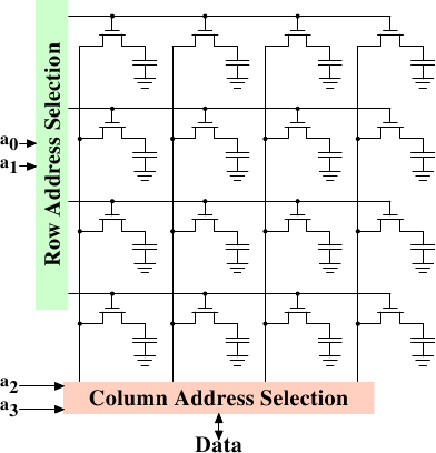
Figure 2.7 shows a DRAM chip at a very high level. The DRAM cells are organized in rows and columns. They could all be aligned in one row but then the DRAM chip would need a huge demultiplexer. With the array approach the design can get by with one demultiplexer and one multiplexer of half the size. {Multiplexers and demultiplexers are equivalent and the multiplexer here needs to work as a demultiplexer when writing. So we will drop the differentiation from now on.} This is a huge saving on all fronts. In the example the address linesa0anda1through the row address selection (RAS) demultiplexer select the address lines of a whole row of cells. When reading, the content of all cells is thusly made available to the column address selection (CAS) {The line over the name indicates that the signal is negated} multiplexer. Based on the address linesa2anda3the content of one column is then made available to the data pin of the DRAM chip. This happens many times in parallel on a number of DRAM chips to produce a total number of bits corresponding to the width of the data bus. |
译者信息
但如果许多的单元生成这种方法不在适合。一个1G的芯片容量(我反感那些SI前缀,对于我一个giga-bit将总是230 而不是109字节)将需要30地址行和230 选项行。一个路由器的大小及许多的输入行以指数方式递增当速度不被牺牲时。一个30地址行路由器需要一大堆芯片的真实身份另外路由器也就复杂起来了。更重要的是,传递30脉冲在地址行同步要比仅仅传递15脉冲困难的多。较少列能精确布局相同长度或恰当的时机(现代DRAM类型像DDR3能自动调整时序但这个限制能让他什么都能忍受)
图2.7展示了一个很高级别的一个DRAM芯片,DRAM被组织在行和列里。他们能在一行中对奇但DRAM芯片需要一个大的路由器。通过阵列方法设计能被一个路由器和一个半的multiplexer获得{多路复用器(multiplexer)和路由器是一样的,这的multiplexer需要以路由器身份工作当写数据时候。那么从现在开始我们开始讨论其区别.}这在所有方面会是一个大的存储。例如地址linesa0和a1通过行地址选择路由器来选择整个行的芯片的地址列,当读的时候,所有的芯片目录能使其纵列选择路由器可用,依据地址linesa2和a3一个纵列的目录用于数据DRAM芯片的接口类型。这发生了许多次在许多DRAM芯片产生一个总记录数的字节匹配给一个宽范围的数据总线。 |
||||||||||||||||||||||||||||||||||||||||||||||||||||||||||||
|
For writing, the new cell value is put on the data bus and, when the cell is selected using theRASandCAS, it is stored in the cell. A pretty straightforward design. There are in reality — obviously — many more complications. There need to be specifications for how much delay there is after the signal before the data will be available on the data bus for reading. The capacitors do not unload instantaneously, as described in the previous section. The signal from the cells is so weak that it needs to be amplified. For writing it must be specified how long the data must be available on the bus after theRASandCASis done to successfully store the new value in the cell (again, capacitors do not fill or drain instantaneously). These timing constants are crucial for the performance of the DRAM chip. We will talk about this in the next section. A secondary scalability problem is that having 30 address lines connected to every RAM chip is not feasible either. Pins of a chip are a precious resources. It is “bad” enough that the data must be transferred as much as possible in parallel (e.g., in 64 bit batches). The memory controller must be able to address each RAM module (collection of RAM chips). If parallel access to multiple RAM modules is required for performance reasons and each RAM module requires its own set of 30 or more address lines, then the memory controller needs to have, for 8 RAM modules, a whopping 240+ pins only for the address handling. |
译者信息
对于写操作,内存单元的数据新值被放到了数据总线,当使用RAS和CAS方式选中内存单元时,数据是存放在内存单元内的。这是一个相当直观的设计,在现实中——很显然——会复杂得多,对于读,需要规范从发出信号到数据在数据总线上变得可读的时延。电容不会像前面章节里面描述的那样立刻自动放电,从内存单元发出的信号是如此这微弱以至于它需要被放大。对于写,必须规范从数据RAS和CAS操作完成后到数据成功的被写入内存单元的时延(当然,电容不会立刻自动充电和放电)。这些时间常量对于DRAM芯片的性能是至关重要的,我们将在下章讨论它。 另一个关于伸缩性的问题是,用30根地址线连接到每一个RAM芯片是行不通的。芯片的针脚是非常珍贵的资源,以至数据必须能并行传输就并行传输(比如:64位为一组)。内存控制器必须有能力解析每一个RAM模块(RAM芯片集合)。如果因为性能的原因要求并发行访问多个RAM模块并且每个RAM模块需要自己独占的30或多个地址线,那么对于8个RAM模块,仅仅是解析地址,内存控制器就需要240+之多的针脚。 |
||||||||||||||||||||||||||||||||||||||||||||||||||||||||||||
|
To counter these secondary scalability problems DRAM chips have, for a long time, multiplexed the address itself. That means the address is transferred in two parts. The first part consisting of address bitsa0anda1in the example in Figure 2.7) select the row. This selection remains active until revoked. Then the second part, address bitsa2anda3, select the column. The crucial difference is that only two external address lines are needed. A few more lines are needed to indicate when theRASandCASsignals are available but this is a small price to pay for cutting the number of address lines in half. This address multiplexing brings its own set of problems, though. We will discuss them in Section 2.2. |
译者信息在很长一段时间里,地址线被复用以解决DRAM芯片的这些次要的可扩展性问题。这意味着地址被转换成两部分。第一部分由地址位a0和a1选择行(如图2.7)。这个选择保持有效直到撤销。然后是第二部分,地址位a2和a3选择列。关键差别在于:只需要两根外部地址线。需要一些很少的线指明RAS和CAS信号有效,但是把地址线的数目减半所付出的代价更小。可是地址复用也带来自身的一些问题。我们将在2.2章中提到。 |
||||||||||||||||||||||||||||||||||||||||||||||||||||||||||||
|
2.1.4 Conclusions Do not worry if the details in this section are a bit overwhelming. The important things to take away from this section are:
The following section will go into more details about the actual process of accessing DRAM memory. We are not going into more details of accessing SRAM, which is usually directly addressed. This happens for speed and because the SRAM memory is limited in size. SRAM is currently used in CPU caches and on-die where the connections are small and fully under control of the CPU designer. CPU caches are a topic which we discuss later but all we need to know is that SRAM cells have a certain maximum speed which depends on the effort spent on the SRAM. The speed can vary from only slightly slower than the CPU core to one or two orders of magnitude slower. |
译者信息
2.1.4 总结 如果这章节的内容有些难以应付,不用担心。纵观这章节的重点,有:
|
||||||||||||||||||||||||||||||||||||||||||||||||||||||||||||
2.2 DRAM Access Technical DetailsIn the section introducing DRAM we saw that DRAM chips multiplex the addresses in order to save resources. We also saw that accessing DRAM cells takes time since the capacitors in those cells do not discharge instantaneously to produce a stable signal; we also saw that DRAM cells must be refreshed. Now it is time to put this all together and see how all these factors determine how the DRAM access has to happen. We will concentrate on current technology; we will not discuss asynchronous DRAM and its variants as they are simply not relevant anymore. Readers interested in this topic are referred to [highperfdram] and [arstechtwo]. We will also not talk about Rambus DRAM (RDRAM) even though the technology is not obsolete. It is just not widely used for system memory. We will concentrate exclusively on Synchronous DRAM (SDRAM) and its successors Double Data Rate DRAM (DDR). |
译者信息
2.2 DRAM访问细节在上文介绍DRAM的时候,我们已经看到DRAM芯片为了节约资源,对地址进行了复用。而且,访问DRAM单元是需要一些时间的,因为电容器的放电并不是瞬时的。此外,我们还看到,DRAM需要不停地刷新。在这一节里,我们将把这些因素拼合起来,看看它们是如何决定DRAM的访问过程。 我们将主要关注在当前的科技上,不会再去讨论异步DRAM以及它的各种变体。如果对它感兴趣,可以去参考[highperfdram]及[arstechtwo]。我们也不会讨论Rambus DRAM(RDRAM),虽然它并不过时,但在系统内存领域应用不广。我们将主要介绍同步DRAM(SDRAM)及其后继者双倍速DRAM(DDR)。 |
||||||||||||||||||||||||||||||||||||||||||||||||||||||||||||
|
Synchronous DRAM, as the name suggests, works relative to a time source. The memory controller provides a clock, the frequency of which determines the speed of the Front Side Bus (FSB) — the memory controller interface used by the DRAM chips. As of this writing, frequencies of 800MHz, 1,066MHz, or even 1,333MHz are available with higher frequencies (1,600MHz) being announced for the next generation. This does not mean the frequency used on the bus is actually this high. Instead, today's buses are double- or quad-pumped, meaning that data is transported two or four times per cycle. Higher numbers sell so the manufacturers like to advertise a quad-pumped 200MHz bus as an “effective” 800MHz bus. For SDRAM today each data transfer consists of 64 bits — 8 bytes. The transfer rate of the FSB is therefore 8 bytes multiplied by the effective bus frequency (6.4GB/s for the quad-pumped 200MHz bus). That sounds a lot but it is the burst speed, the maximum speed which will never be surpassed. As we will see now the protocol for talking to the RAM modules has a lot of downtime when no data can be transmitted. It is exactly this downtime which we must understand and minimize to achieve the best performance. |
译者信息
同步DRAM,顾名思义,是参照一个时间源工作的。由内存控制器提供一个时钟,时钟的频率决定了前端总线(FSB)的速度。FSB是内存控制器提供给DRAM芯片的接口。在我写作本文的时候,FSB已经达到800MHz、1066MHz,甚至1333MHz,并且下一代的1600MHz也已经宣布。但这并不表示时钟频率有这么高。实际上,目前的总线都是双倍或四倍传输的,每个周期传输2次或4次数据。报的越高,卖的越好,所以这些厂商们喜欢把四倍传输的200MHz总线宣传为“有效的”800MHz总线。 以今天的SDRAM为例,每次数据传输包含64位,即8字节。所以FSB的传输速率应该是有效总线频率乘于8字节(对于4倍传输200MHz总线而言,传输速率为6.4GB/s)。听起来很高,但要知道这只是峰值速率,实际上无法达到的最高速率。我们将会看到,与RAM模块交流的协议有大量时间是处于非工作状态,不进行数据传输。我们必须对这些非工作时间有所了解,并尽量缩短它们,才能获得最佳的性能。 |
||||||||||||||||||||||||||||||||||||||||||||||||||||||||||||
|
2.2.1 Read Access Protocol
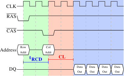
Figure 2.8 shows the activity on some of the connectors of a DRAM module which happens in three differently colored phases. As usual, time flows from left to right. A lot of details are left out. Here we only talk about the bus clock,RASandCASsignals, and the address and data buses. A read cycle begins with the memory controller making the row address available on the address bus and lowering theRASsignal. All signals are read on the rising edge of the clock (CLK) so it does not matter if the signal is not completely square as long as it is stable at the time it is read. Setting the row address causes the RAM chip to start latching the addressed row. TheCASsignal can be sent aftertRCD(RAS-to-CASDelay) clock cycles. The column address is then transmitted by making it available on the address bus and lowering theCASline. Here we can see how the two parts of the address (more or less halves, nothing else makes sense) can be transmitted over the same address bus. |
译者信息
2.2.1 读访问协议
图2.8展示了某个DRAM模块一些连接器上的活动,可分为三个阶段,图上以不同颜色表示。按惯例,时间为从左向右流逝。这里忽略了许多细节,我们只关注时钟频率、RAS与CAS信号、地址总线和数据总线。首先,内存控制器将行地址放在地址总线上,并降低RAS信号,读周期开始。所有信号都在时钟(CLK)的上升沿读取,因此,只要信号在读取的时间点上保持稳定,就算不是标准的方波也没有关系。设置行地址会促使RAM芯片锁住指定的行。 CAS信号在tRCD(RAS到CAS时延)个时钟周期后发出。内存控制器将列地址放在地址总线上,降低CAS线。这里我们可以看到,地址的两个组成部分是怎么通过同一条总线传输的。 |
||||||||||||||||||||||||||||||||||||||||||||||||||||||||||||
|
Now the addressing is complete and the data can be transmitted. The RAM chip needs some time to prepare for this. The delay is usually calledCASLatency (CL). In Figure 2.8 theCASlatency is 2. It can be higher or lower, depending on the quality of the memory controller, motherboard, and DRAM module. The latency can also have half values. With CL=2.5 the first data would be available at the first falling flank in the blue area. With all this preparation to get to the data it would be wasteful to only transfer one data word. This is why DRAM modules allow the memory controller to specify how much data is to be transmitted. Often the choice is between 2, 4, or 8 words. This allows filling entire lines in the caches without a newRAS/CASsequence. It is also possible for the memory controller to send a newCASsignal without resetting the row selection. In this way, consecutive memory addresses can be read from or written to significantly faster because theRASsignal does not have to be sent and the row does not have to be deactivated (see below). Keeping the row “open” is something the memory controller has to decide. Speculatively leaving it open all the time has disadvantages with real-world applications (see [highperfdram]). Sending newCASsignals is only subject to the Command Rate of the RAM module (usually specified as Tx, where x is a value like 1 or 2; it will be 1 for high-performance DRAM modules which accept new commands every cycle). In this example the SDRAM spits out one word per cycle. This is what the first generation does. DDR is able to transmit two words per cycle. This cuts down on the transfer time but does not change the latency. In principle, DDR2 works the same although in practice it looks different. There is no need to go into the details here. It is sufficient to note that DDR2 can be made faster, cheaper, more reliable, and is more energy efficient (see [ddrtwo] for more information). |
译者信息
至此,寻址结束,是时候传输数据了。但RAM芯片任然需要一些准备时间,这个时间称为CAS时延(CL)。在图2.8中CL为2。这个值可大可小,它取决于内存控制器、主板和DRAM模块的质量。CL还可能是半周期。假设CL为2.5,那么数据将在蓝色区域内的第一个下降沿准备就绪。 既然数据的传输需要这么多的准备工作,仅仅传输一个字显然是太浪费了。因此,DRAM模块允许内存控制指定本次传输多少数据。可以是2、4或8个字。这样,就可以一次填满高速缓存的整条线,而不需要额外的RAS/CAS序列。另外,内存控制器还可以在不重置行选择的前提下发送新的CAS信号。这样,读取或写入连续的地址就可以变得非常快,因为不需要发送RAS信号,也不需要把行置为非激活状态(见下文)。是否要将行保持为“打开”状态是内存控制器判断的事情。让它一直保持打开的话,对真正的应用会有不好的影响(参见[highperfdram])。CAS信号的发送仅与RAM模块的命令速率(Command Rate)有关(常常记为Tx,其中x为1或2,高性能的DRAM模块一般为1,表示在每个周期都可以接收新命令)。 在上图中,SDRAM的每个周期输出一个字的数据。这是第一代的SDRAM。而DDR可以在一个周期中输出两个字。这种做法可以减少传输时间,但无法降低时延。DDR2尽管看上去不同,但在本质上也是相同的做法。对于DDR2,不需要再深入介绍了,我们只需要知道DDR2更快、更便宜、更可靠、更节能(参见[ddrtwo])就足够了。 |
||||||||||||||||||||||||||||||||||||||||||||||||||||||||||||
|
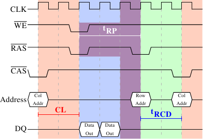
2.2.2 Precharge and Activation Figure 2.8 does not cover the whole cycle. It only shows parts of the full cycle of accessing DRAM. Before a newRASsignal can be sent the currently latched row must be deactivated and the new row must be precharged. We can concentrate here on the case where this is done with an explicit command. There are improvements to the protocol which, in some situations, allows this extra step to be avoided. The delays introduced by precharging still affect the operation, though.
Figure 2.9 shows the activity starting from oneCASsignal to theCASsignal for another row. The data requested with the firstCASsignal is available as before, after CL cycles. In the example two words are requested which, on a simple SDRAM, takes two cycles to transmit. Alternatively, imagine four words on a DDR chip. |
译者信息
2.2.2 预充电与激活图2.8并不完整,它只画出了访问DRAM的完整循环的一部分。在发送RAS信号之前,必须先把当前锁住的行置为非激活状态,并对新行进行预充电。在这里,我们主要讨论由于显式发送指令而触发以上行为的情况。协议本身作了一些改进,在某些情况下是可以省略这个步骤的,但预充电带来的时延还是会影响整个操作。
图2.9显示的是两次CAS信号的时序图。第一次的数据在CL周期后准备就绪。图中的例子里,是在SDRAM上,用两个周期传输了两个字的数据。如果换成DDR的话,则可以传输4个字。 |
||||||||||||||||||||||||||||||||||||||||||||||||||||||||||||
|
Even on DRAM modules with a command rate of one the precharge command cannot be issued right away. It is necessary to wait as long as it takes to transmit the data. In this case it takes two cycles. This happens to be the same as CL but that is just a coincidence. The precharge signal has no dedicated line; instead, some implementations issue it by lowering the Write Enable (WE) andRASline simultaneously. This combination has no useful meaning by itself (see [micronddr] for encoding details). Once the precharge command is issued it takestRP(Row Precharge time) cycles until the row can be selected. In Figure 2.9 much of the time (indicated by the purplish color) overlaps with the memory transfer (light blue). This is good! ButtRPis larger than the transfer time and so the nextRASsignal is stalled for one cycle. |
译者信息
即使是在一个命令速率为1的DRAM模块上,也无法立即发出预充电命令,而要等数据传输完成。在上图中,即为两个周期。刚好与CL相同,但只是巧合而已。预充电信号并没有专用线,某些实现是用同时降低写使能(WE)线和RAS线的方式来触发。这一组合方式本身没有特殊的意义(参见[micronddr])。 发出预充电信命令后,还需等待tRP(行预充电时间)个周期之后才能使行被选中。在图2.9中,这个时间(紫色部分)大部分与内存传输的时间(淡蓝色部分)重合。不错。但tRP大于传输时间,因此下一个RAS信号只能等待一个周期。 |
||||||||||||||||||||||||||||||||||||||||||||||||||||||||||||
|
If we were to continue the timeline in the diagram we would find that the next data transfer happens 5 cycles after the previous one stops. This means the data bus is only in use two cycles out of seven. Multiply this with the FSB speed and the theoretical 6.4GB/s for a 800MHz bus become 1.8GB/s. That is bad and must be avoided. The techniques described in Section 6 help to raise this number. But the programmer usually has to do her share. There is one more timing value for a SDRAM module which we have not discussed. In Figure 2.9 the precharge command was only limited by the data transfer time. Another constraint is that an SDRAM module needs time after aRASsignal before it can precharge another row (denoted astRAS). This number is usually pretty high, in the order of two or three times thetRPvalue. This is a problem if, after aRASsignal, only oneCASsignal follows and the data transfer is finished in a few cycles. Assume that in Figure 2.9 the initialCASsignal was preceded directly by aRASsignal and thattRASis 8 cycles. Then the precharge command would have to be delayed by one additional cycle since the sum oftRCD, CL, andtRP(since it is larger than the data transfer time) is only 7 cycles. |
译者信息
如果我们补充完整上图中的时间线,最后会发现下一次数据传输发生在前一次的5个周期之后。这意味着,数据总线的7个周期中只有2个周期才是真正在用的。再用它乘于FSB速度,结果就是,800MHz总线的理论速率6.4GB/s降到了1.8GB/s。真是太糟了。第6节将介绍一些技术,可以帮助我们提高总线有效速率。程序员们也需要尽自己的努力。 SDRAM还有一些定时值,我们并没有谈到。在图2.9中,预充电命令仅受制于数据传输时间。除此之外,SDRAM模块在RAS信号之后,需要经过一段时间,才能进行预充电(记为tRAS)。它的值很大,一般达到tRP的2到3倍。如果在某个RAS信号之后,只有一个CAS信号,而且数据只传输很少几个周期,那么就有问题了。假设在图2.9中,第一个CAS信号是直接跟在一个RAS信号后免的,而tRAS为8个周期。那么预充电命令还需要被推迟一个周期,因为tRCD、CL和tRP加起来才7个周期。 |
||||||||||||||||||||||||||||||||||||||||||||||||||||||||||||
|
DDR modules are often described using a special notation: w-x-y-z-T. For instance: 2-3-2-8-T1. This means:
There are numerous other timing constants which affect the way commands can be issued and are handled. Those five constants are in practice sufficient to determine the performance of the module, though. It is sometimes useful to know this information for the computers in use to be able to interpret certain measurements. It is definitely useful to know these details when buying computers since they, along with the FSB and SDRAM module speed, are among the most important factors determining a computer's speed. The very adventurous reader could also try to tweak a system. Sometimes the BIOS allows changing some or all these values. SDRAM modules have programmable registers where these values can be set. Usually the BIOS picks the best default value. If the quality of the RAM module is high it might be possible to reduce the one or the other latency without affecting the stability of the computer. Numerous overclocking websites all around the Internet provide ample of documentation for doing this. Do it at your own risk, though and do not say you have not been warned. |
译者信息
DDR模块往往用w-z-y-z-T来表示。例如,2-3-2-8-T1,意思是: w 2 CAS时延(CL) 当然,除以上的参数外,还有许多其它参数影响命令的发送与处理。但以上5个参数已经足以确定模块的性能。 在解读计算机性能参数时,这些信息可能会派上用场。而在购买计算机时,这些信息就更有用了,因为它们与FSB/SDRAM速度一起,都是决定计算机速度的关键因素。 喜欢冒险的读者们还可以利用它们来调优系统。有些计算机的BIOS可以让你修改这些参数。SDRAM模块有一些可编程寄存器,可供设置参数。BIOS一般会挑选最佳值。如果RAM模块的质量足够好,我们可以在保持系统稳定的前提下将减小以上某个时延参数。互联网上有大量超频网站提供了相关的文档。不过,这是有风险的,需要大家自己承担,可别怪我没有事先提醒哟。 |
||||||||||||||||||||||||||||||||||||||||||||||||||||||||||||
|
2.2.3 Recharging A mostly-overlooked topic when it comes to DRAM access is recharging. As explained in Section 2.1.2, DRAM cells must constantly be refreshed. This does not happen completely transparently for the rest of the system. At times when a row {Rows are the granularity this happens with despite what [highperfdram] and other literature says (see [micronddr]).} is recharged no access is possible. The study in [highperfdram] found that “[s]urprisingly, DRAM refresh organization can affect performance dramatically”. Each DRAM cell must be refreshed every 64ms according to the JEDEC specification. If a DRAM array has 8,192 rows this means the memory controller has to issue a refresh command on average every 7.8125µs (refresh commands can be queued so in practice the maximum interval between two requests can be higher). It is the memory controller's responsibility to schedule the refresh commands. The DRAM module keeps track of the address of the last refreshed row and automatically increases the address counter for each new request. There is really not much the programmer can do about the refresh and the points in time when the commands are issued. But it is important to keep this part to the DRAM life cycle in mind when interpreting measurements. If a critical word has to be retrieved from a row which currently is being refreshed the processor could be stalled for quite a long time. How long each refresh takes depends on the DRAM module. |
译者信息
2.2.3 重充电谈到DRAM的访问时,重充电是常常被忽略的一个主题。在2.1.2中曾经介绍,DRAM必须保持刷新。……行在充电时是无法访问的。[highperfdram]的研究发现,“令人吃惊,DRAM刷新对性能有着巨大的影响”。 根据JEDEC规范,DRAM单元必须保持每64ms刷新一次。对于8192行的DRAM,这意味着内存控制器平均每7.8125µs就需要发出一个刷新命令(在实际情况下,由于刷新命令可以纳入队列,因此这个时间间隔可以更大一些)。刷新命令的调度由内存控制器负责。DRAM模块会记录上一次刷新行的地址,然后在下次刷新请求时自动对这个地址进行递增。 对于刷新及发出刷新命令的时间点,程序员无法施加影响。但我们在解读性能参数时有必要知道,它也是DRAM生命周期的一个部分。如果系统需要读取某个重要的字,而刚好它所在的行正在刷新,那么处理器将会被延迟很长一段时间。刷新的具体耗时取决于DRAM模块本身。 |
||||||||||||||||||||||||||||||||||||||||||||||||||||||||||||
|
2.2.4 Memory Types It is worth spending some time on the current and soon-to-be current memory types in use. We will start with SDR (Single Data Rate) SDRAMs since they are the basis of the DDR (Double Data Rate) SDRAMs. SDRs were pretty simple. The memory cells and the data transfer rate were identical.
In Figure 2.10 the DRAM cell array can output the memory content at the same rate it can be transported over the memory bus. If the DRAM cell array can operate at 100MHz, the data transfer rate of the bus is thus 100Mb/s. The frequency f for all components is the same. Increasing the throughput of the DRAM chip is expensive since the energy consumption rises with the frequency. With a huge number of array cells this is prohibitively expensive. {Power = Dynamic Capacity × Voltage2 × Frequency.} In reality it is even more of a problem since increasing the frequency usually also requires increasing the voltage to maintain stability of the system. DDR SDRAM (called DDR1 retroactively) manages to improve the throughput without increasing any of the involved frequencies.
|
译者信息
2.2.4 内存类型我们有必要花一些时间来了解一下目前流行的内存,以及那些即将流行的内存。首先从SDR(单倍速)SDRAM开始,因为它们是DDR(双倍速)SDRAM的基础。SDR非常简单,内存单元和数据传输率是相等的。
在图2.10中,DRAM单元阵列能以等同于内存总线的速率输出内容。假设DRAM单元阵列工作在100MHz上,那么总线的数据传输率可以达到100Mb/s。所有组件的频率f保持相同。由于提高频率会导致耗电量增加,所以提高吞吐量需要付出很高的的代价。如果是很大规模的内存阵列,代价会非常巨大。{功率 = 动态电容 x 电压2 x 频率}。而且,提高频率还需要在保持系统稳定的情况下提高电压,这更是一个问题。因此,就有了DDR SDRAM(现在叫DDR1),它可以在不提高频率的前提下提高吞吐量。
|
||||||||||||||||||||||||||||||||||||||||||||||||||||||||||||
| The difference between SDR and DDR1 is, as can be seen in Figure 2.11 and guessed from the name, that twice the amount of data is transported per cycle. I.e., the DDR1 chip transports data on the rising and falling edge. This is sometimes called a “double-pumped” bus. To make this possible without increasing the frequency of the cell array a buffer has to be introduced. This buffer holds two bits per data line. This in turn requires that, in the cell array in Figure 2.7, the data bus consists of two lines. Implementing this is trivial: one only has the use the same column address for two DRAM cells and access them in parallel. The changes to the cell array to implement this are also minimal.
The SDR DRAMs were known simply by their frequency (e.g., PC100 for 100MHz SDR). To make DDR1 DRAM sound better the marketers had to come up with a new scheme since the frequency did not change. They came with a name which contains the transfer rate in bytes a DDR module (they have 64-bit busses) can sustain: 100MHz × 64bit × 2 = 1,600MB/s |
译者信息
我们从图2.11上可以看出DDR1与SDR的不同之处,也可以从DDR1的名字里猜到那么几分,DDR1的每个周期可以传输两倍的数据,它的上升沿和下降沿都传输数据。有时又被称为“双泵(double-pumped)”总线。为了在不提升频率的前提下实现双倍传输,DDR引入了一个缓冲区。缓冲区的每条数据线都持有两位。它要求内存单元阵列的数据总线包含两条线。实现的方式很简单,用同一个列地址同时访问两个DRAM单元。对单元阵列的修改也很小。 SDR DRAM是以频率来命名的(例如,对应于100MHz的称为PC100)。为了让DDR1听上去更好听,营销人员们不得不想了一种新的命名方案。这种新方案中含有DDR模块可支持的传输速率(DDR拥有64位总线): 100MHz x 64位 x 2 = 1600MB/s |
||||||||||||||||||||||||||||||||||||||||||||||||||||||||||||
Hence a DDR module with 100MHz frequency is called PC1600. With 1600 > 100 all marketing requirements are fulfilled; it sounds much better although the improvement is really only a factor of two. { I will take the factor of two but I do not have to like the inflated numbers.}
To get even more out of the memory technology DDR2 includes a bit more innovation. The most obvious change that can be seen in Figure 2.12 is the doubling of the frequency of the bus. Doubling the frequency means doubling the bandwidth. Since this doubling of the frequency is not economical for the cell array it is now required that the I/O buffer gets four bits in each clock cycle which it then can send on the bus. This means the changes to the DDR2 modules consist of making only the I/O buffer component of the DIMM capable of running at higher speeds. This is certainly possible and will not require measurably more energy, it is just one tiny component and not the whole module. The names the marketers came up with for DDR2 are similar to the DDR1 names only in the computation of the value the factor of two is replaced by four (we now have a quad-pumped bus). Figure 2.13 shows the names of the modules in use today.
|
译者信息
于是,100MHz频率的DDR模块就被称为PC1600。由于1600 > 100,营销方面的需求得到了满足,听起来非常棒,但实际上仅仅只是提升了两倍而已。{我接受两倍这个事实,但不喜欢类似的数字膨胀戏法。}
为了更进一步,DDR2有了更多的创新。在图2.12中,最明显的变化是,总线的频率加倍了。频率的加倍意味着带宽的加倍。如果对单元阵列的频率加倍,显然是不经济的,因此DDR2要求I/O缓冲区在每个时钟周期读取4位。也就是说,DDR2的变化仅在于使I/O缓冲区运行在更高的速度上。这是可行的,而且耗电也不会显著增加。DDR2的命名与DDR1相仿,只是将因子2替换成4(四泵总线)。图2.13显示了目前常用的一些模块的名称。
|
||||||||||||||||||||||||||||||||||||||||||||||||||||||||||||
| There is one more twist to the naming. The FSB speed used by CPU, motherboard, and DRAM module is specified by using the effective frequency. I.e., it factors in the transmission on both flanks of the clock cycle and thereby inflates the number. So, a 133MHz module with a 266MHz bus has an FSB “frequency” of 533MHz.
The specification for DDR3 (the real one, not the fake GDDR3 used in graphics cards) calls for more changes along the lines of the transition to DDR2. The voltage will be reduced from 1.8V for DDR2 to 1.5V for DDR3. Since the power consumption equation is calculated using the square of the voltage this alone brings a 30% improvement. Add to this a reduction in die size plus other electrical advances and DDR3 can manage, at the same frequency, to get by with half the power consumption. Alternatively, with higher frequencies, the same power envelope can be hit. Or with double the capacity the same heat emission can be achieved. |
译者信息
在命名方面还有一个拧巴的地方。FSB速度是用有效频率来标记的,即把上升、下降沿均传输数据的因素考虑进去,因此数字被撑大了。所以,拥有266MHz总线的133MHz模块有着533MHz的FSB“频率”。 DDR3要求更多的改变(这里指真正的DDR3,而不是图形卡中假冒的GDDR3)。电压从1.8V下降到1.5V。由于耗电是与电压的平方成正比,因此可以节约30%的电力。加上管芯(die)的缩小和电气方面的其它进展,DDR3可以在保持相同频率的情况下,降低一半的电力消耗。或者,在保持相同耗电的情况下,达到更高的频率。又或者,在保持相同热量排放的情况下,实现容量的翻番。 |
||||||||||||||||||||||||||||||||||||||||||||||||||||||||||||
|
The cell array of DDR3 modules will run at a quarter of the speed of the external bus which requires an 8 bit I/O buffer, up from 4 bits for DDR2. See Figure 2.14 for the schematics.
Initially DDR3 modules will likely have slightly higherCASlatencies just because the DDR2 technology is more mature. This would cause DDR3 to be useful only at frequencies which are higher than those which can be achieved with DDR2, and, even then, mostly when bandwidth is more important than latency. There is already talk about 1.3V modules which can achieve the sameCASlatency as DDR2. In any case, the possibility of achieving higher speeds because of faster buses will outweigh the increased latency. |
译者信息
DDR3模块的单元阵列将运行在内部总线的四分之一速度上,DDR3的I/O缓冲区从DDR2的4位提升到8位。见图2.14。
一开始,DDR3可能会有较高的CAS时延,因为DDR2的技术相比之下更为成熟。由于这个原因,DDR3可能只会用于DDR2无法达到的高频率下,而且带宽比时延更重要的场景。此前,已经有讨论指出,1.3V的DDR3可以达到与DDR2相同的CAS时延。无论如何,更高速度带来的价值都会超过时延增加带来的影响。 |
||||||||||||||||||||||||||||||||||||||||||||||||||||||||||||
|
One possible problem with DDR3 is that, for 1,600Mb/s transfer rate or higher, the number of modules per channel may be reduced to just one. In earlier versions this requirement held for all frequencies, so one can hope that the requirement will at some point be lifted for all frequencies. Otherwise the capacity of systems will be severely limited. Figure 2.15 shows the names of the expected DDR3 modules. JEDEC agreed so far on the first four types. Given that Intel's 45nm processors have an FSB speed of 1,600Mb/s, the 1,866Mb/s is needed for the overclocking market. We will likely see more of this towards the end of the DDR3 lifecycle.
|
译者信息
DDR3可能会有一个问题,即在1600Mb/s或更高速率下,每个通道的模块数可能会限制为1。在早期版本中,这一要求是针对所有频率的。我们希望这个要求可以提高一些,否则系统容量将会受到严重的限制。 图2.15显示了我们预计中各DDR3模块的名称。JEDEC目前同意了前四种。由于Intel的45nm处理器是1600Mb/s的FSB,1866Mb/s可以用于超频市场。随着DDR3的发展,可能会有更多类型加入。
|
||||||||||||||||||||||||||||||||||||||||||||||||||||||||||||
| All DDR memory has one problem: the increased bus frequency makes it hard to create parallel data busses. A DDR2 module has 240 pins. All connections to data and address pins must be routed so that they have approximately the same length. Even more of a problem is that, if more than one DDR module is to be daisy-chained on the same bus, the signals get more and more distorted for each additional module. The DDR2 specification allow only two modules per bus (aka channel), the DDR3 specification only one module for high frequencies. With 240 pins per channel a single Northbridge cannot reasonably drive more than two channels. The alternative is to have external memory controllers (as in Figure 2.2) but this is expensive.
What this means is that commodity motherboards are restricted to hold at most four DDR2 or DDR3 modules. This restriction severely limits the amount of memory a system can have. Even old 32-bit IA-32 processors can handle 64GB of RAM and memory demand even for home use is growing, so something has to be done. |
译者信息
所有的DDR内存都有一个问题:不断增加的频率使得建立并行数据总线变得十分困难。一个DDR2模块有240根引脚。所有到地址和数据引脚的连线必须被布置得差不多一样长。更大的问题是,如果多于一个DDR模块通过菊花链连接在同一个总线上,每个模块所接收到的信号随着模块的增加会变得越来越扭曲。DDR2规范允许每条总线(又称通道)连接最多两个模块,DDR3在高频率下只允许每个通道连接一个模块。每条总线多达240根引脚使得单个北桥无法以合理的方式驱动两个通道。替代方案是增加外部内存控制器(如图2.2),但这会提高成本。 这意味着商品主板所搭载的DDR2或DDR3模块数将被限制在最多四条,这严重限制了系统的最大内存容量。即使是老旧的32位IA-32处理器也可以使用64GB内存。即使是家庭对内存的需求也在不断增长,所以,某些事必须开始做了。 |
||||||||||||||||||||||||||||||||||||||||||||||||||||||||||||
|
One answer is to add memory controllers into each processor as explained in Section 2. AMD does it with the Opteron line and Intel will do it with their CSI technology. This will help as long as the reasonable amount of memory a processor is able to use can be connected to a single processor. In some situations this is not the case and this setup will introduce a NUMA architecture and its negative effects. For some situations another solution is needed. Intel's answer to this problem for big server machines, at least for the next years, is called Fully Buffered DRAM (FB-DRAM). The FB-DRAM modules use the same components as today's DDR2 modules which makes them relatively cheap to produce. The difference is in the connection with the memory controller. Instead of a parallel data bus FB-DRAM utilizes a serial bus (Rambus DRAM had this back when, too, and SATA is the successor of PATA, as is PCI Express for PCI/AGP). The serial bus can be driven at a much higher frequency, reverting the negative impact of the serialization and even increasing the bandwidth. The main effects of using a serial bus are
|
译者信息
一种解法是,在处理器中加入内存控制器,我们在第2节中曾经介绍过。AMD的Opteron系列和Intel的CSI技术就是采用这种方法。只要我们能把处理器要求的内存连接到处理器上,这种解法就是有效的。如果不能,按照这种思路就会引入NUMA架构,当然同时也会引入它的缺点。而在有些情况下,我们需要其它解法。 Intel针对大型服务器方面的解法(至少在未来几年),是被称为全缓冲DRAM(FB-DRAM)的技术。FB-DRAM采用与DDR2相同的器件,因此造价低廉。不同之处在于它们与内存控制器的连接方式。FB-DRAM没有用并行总线,而用了串行总线(Rambus DRAM had this back when, too, 而SATA是PATA的继任者,就像PCI Express是PCI/AGP的继承人一样)。串行总线可以达到更高的频率,串行化的负面影响,甚至可以增加带宽。使用串行总线后
|
||||||||||||||||||||||||||||||||||||||||||||||||||||||||||||
| An FB-DRAM module has only 69 pins, compared with the 240 for DDR2. Daisy chaining FB-DRAM modules is much easier since the electrical effects of the bus can be handled much better. The FB-DRAM specification allows up to 8 DRAM modules per channel.
Compared with the connectivity requirements of a dual-channel Northbridge it is now possible to drive 6 channels of FB-DRAM with fewer pins: 2×240 pins versus 6×69 pins. The routing for each channel is much simpler which could also help reducing the cost of the motherboards. Fully duplex parallel busses are prohibitively expensive for the traditional DRAM modules, duplicating all those lines is too costly. With serial lines (even if they are differential, as FB-DRAM requires) this is not the case and so the serial bus is designed to be fully duplexed, which means, in some situations, that the bandwidth is theoretically doubled alone by this. But it is not the only place where parallelism is used for bandwidth increase. Since an FB-DRAM controller can run up to six channels at the same time the bandwidth can be increased even for systems with smaller amounts of RAM by using FB-DRAM. Where a DDR2 system with four modules has two channels, the same capacity can handled via four channels using an ordinary FB-DRAM controller. The actual bandwidth of the serial bus depends on the type of DDR2 (or DDR3) chips used on the FB-DRAM module. |
译者信息
FB-DRAM只有69个脚。通过菊花链方式连接多个FB-DRAM也很简单。FB-DRAM规范允许每个通道连接最多8个模块。 在对比下双通道北桥的连接性,采用FB-DRAM后,北桥可以驱动6个通道,而且脚数更少——6x69对比2x240。每个通道的布线也更为简单,有助于降低主板的成本。 全双工的并行总线过于昂贵。而换成串行线后,这不再是一个问题,因此串行总线按全双工来设计的,这也意味着,在某些情况下,仅靠这一特性,总线的理论带宽已经翻了一倍。还不止于此。由于FB-DRAM控制器可同时连接6个通道,因此可以利用它来增加某些小内存系统的带宽。对于一个双通道、4模块的DDR2系统,我们可以用一个普通FB-DRAM控制器,用4通道来实现相同的容量。串行总线的实际带宽取决于在FB-DRAM模块中所使用的DDR2(或DDR3)芯片的类型。 |
||||||||||||||||||||||||||||||||||||||||||||||||||||||||||||
|
We can summarize the advantages like this:
|
译者信息
我们可以像这样总结这些优势: DDR2 FB-DRAM |
||||||||||||||||||||||||||||||||||||||||||||||||||||||||||||
| Pins 240 69 Channels 2 6 DIMMs/Channel 2 8 Max Memory 16GB 192GB Throughput ~10GB/s ~40GB/s
There are a few drawbacks to FB-DRAMs if multiple DIMMs on one channel are used. The signal is delayed—albeit minimally—at each DIMM in the chain, which means the latency increases. But for the same amount of memory with the same frequency FB-DRAM can always be faster than DDR2 and DDR3 since only one DIMM per channel is needed; for large memory systems DDR simply has no answer using commodity components. |
译者信息
如果在单个通道上使用多个DIMM,会有一些问题。信号在每个DIMM上都会有延迟(尽管很小),也就是说,延迟是递增的。不过,如果在相同频率和相同容量上进行比较,FB-DRAM总是能快过DDR2及DDR3,因为FB-DRAM只需要在每个通道上使用一个DIMM即可。而如果说到大型内存系统,那么DDR更是没有商用组件的解决方案。 |
||||||||||||||||||||||||||||||||||||||||||||||||||||||||||||
|
2.2.5 Conclusions This section should have shown that accessing DRAM is not an arbitrarily fast process. At least not fast compared with the speed the processor is running and with which it can access registers and cache. It is important to keep in mind the differences between CPU and memory frequencies. An Intel Core 2 processor running at 2.933GHz and a 1.066GHz FSB have a clock ratio of 11:1 (note: the 1.066GHz bus is quad-pumped). Each stall of one cycle on the memory bus means a stall of 11 cycles for the processor. For most machines the actual DRAMs used are slower, thusly increasing the delay. Keep these numbers in mind when we are talking about stalls in the upcoming sections. The timing charts for the read command have shown that DRAM modules are capable of high sustained data rates. Entire DRAM rows could be transported without a single stall. The data bus could be kept occupied 100%. For DDR modules this means two 64-bit words transferred each cycle. With DDR2-800 modules and two channels this means a rate of 12.8GB/s. But, unless designed this way, DRAM access is not always sequential. Non-continuous memory regions are used which means precharging and newRASsignals are needed. This is when things slow down and when the DRAM modules need help. The sooner the precharging can happen and theRASsignal sent the smaller the penalty when the row is actually used. Hardware and software prefetching (see Section 6.3) can be used to create more overlap in the timing and reduce the stall. Prefetching also helps shift memory operations in time so that there is less contention at later times, right before the data is actually needed. This is a frequent problem when the data produced in one round has to be stored and the data required for the next round has to be read. By shifting the read in time, the write and read operations do not have to be issued at basically the same time. |
译者信息
2.2.5 结论通过本节,大家应该了解到访问DRAM的过程并不是一个快速的过程。至少与处理器的速度相比,或与处理器访问寄存器及缓存的速度相比,DRAM的访问不算快。大家还需要记住CPU和内存的频率是不同的。Intel Core 2处理器运行在2.933GHz,而1.066GHz FSB有11:1的时钟比率(注: 1.066GHz的总线为四泵总线)。那么,内存总线上延迟一个周期意味着处理器延迟11个周期。绝大多数机器使用的DRAM更慢,因此延迟更大。在后续的章节中,我们需要讨论延迟这个问题时,请把以上的数字记在心里。 前文中读命令的时序图表明,DRAM模块可以支持高速数据传输。每个完整行可以被毫无延迟地传输。数据总线可以100%被占。对DDR而言,意味着每个周期传输2个64位字。对于DDR2-800模块和双通道而言,意味着12.8GB/s的速率。 但是,除非是特殊设计,DRAM的访问并不总是串行的。访问不连续的内存区意味着需要预充电和RAS信号。于是,各种速度开始慢下来,DRAM模块急需帮助。预充电的时间越短,数据传输所受的惩罚越小。 硬件和软件的预取(参见第6.3节)可以在时序中制造更多的重叠区,降低延迟。预取还可以转移内存操作的时间,从而减少争用。我们常常遇到的问题是,在这一轮中生成的数据需要被存储,而下一轮的数据需要被读出来。通过转移读取的时间,读和写就不需要同时发出了。 |
||||||||||||||||||||||||||||||||||||||||||||||||||||||||||||
2.3 Other Main Memory UsersBeside the CPUs there are other system components which can access the main memory. High-performance cards such as network and mass-storage controllers cannot afford to pipe all the data they need or provide through the CPU. Instead, they read or write the data directly from/to the main memory (Direct Memory Access, DMA). In Figure 2.1 we can see that the cards can talk through the South- and Northbridge directly with the memory. Other buses, like USB, also require FSB bandwidth—even though they do not use DMA—since the Southbridge is connected to the Northbridge through the FSB, too. While DMA is certainly beneficial, it means that there is more competition for the FSB bandwidth. In times with high DMA traffic the CPU might stall more than usual while waiting for data from the main memory. There are ways around this given the right hardware. With an architecture as in Figure 2.3 one can make sure the computation uses memory on nodes which are not affected by DMA. It is also possible to attach a Southbridge to each node, equally distributing the load on the FSB of all the nodes. There are a myriad of possibilities. In Section 6 we will introduce techniques and programming interfaces which help achieving the improvements which are possible in software. |
译者信息
2.3 主存的其它用户除了CPU外,系统中还有其它一些组件也可以访问主存。高性能网卡或大规模存储控制器是无法承受通过CPU来传输数据的,它们一般直接对内存进行读写(直接内存访问,DMA)。在图2.1中可以看到,它们可以通过南桥和北桥直接访问内存。另外,其它总线,比如USB等也需要FSB带宽,即使它们并不使用DMA,但南桥仍要通过FSB连接到北桥。 DMA当然有很大的优点,但也意味着FSB带宽会有更多的竞争。在有大量DMA流量的情况下,CPU在访问内存时必然会有更大的延迟。我们可以用一些硬件来解决这个问题。例如,通过图2.3中的架构,我们可以挑选不受DMA影响的节点,让它们的内存为我们的计算服务。还可以在每个节点上连接一个南桥,将FSB的负荷均匀地分担到每个节点上。除此以外,还有许多其它方法。我们将在第6节中介绍一些技术和编程接口,它们能够帮助我们通过软件的方式改善这个问题。 |
||||||||||||||||||||||||||||||||||||||||||||||||||||||||||||
|
Finally it should be mentioned that some cheap systems have graphics systems without separate, dedicated video RAM. Those systems use parts of the main memory as video RAM. Since access to the video RAM is frequent (for a 1024x768 display with 16 bpp at 60Hz we are talking 94MB/s) and system memory, unlike RAM on graphics cards, does not have two ports this can substantially influence the systems performance and especially the latency. It is best to ignore such systems when performance is a priority. They are more trouble than they are worth. People buying those machines know they will not get the best performance. Continue to: |
译者信息
最后,还需要提一下某些廉价系统,它们的图形系统没有专用的显存,而是采用主存的一部分作为显存。由于对显存的访问非常频繁(例如,对于1024x768、16bpp、60Hz的显示设置来说,需要95MB/s的数据速率),而主存并不像显卡上的显存,并没有两个端口,因此这种配置会对系统性能、尤其是时延造成一定的影响。如果大家对系统性能要求比较高,最好不要采用这种配置。这种系统带来的问题超过了本身的价值。人们在购买它们时已经做好了性能不佳的心理准备。 继续阅读: |


![[Formulas]](http://static.oschina.net/uploads/img/201302/06104432_i34C.png)


Part 2 CPU Cache
|
CPUs are today much more sophisticated than they were only 25 years ago. In those days, the frequency of the CPU core was at a level equivalent to that of the memory bus. Memory access was only a bit slower than register access. But this changed dramatically in the early 90s, when CPU designers increased the frequency of the CPU core but the frequency of the memory bus and the performance of RAM chips did not increase proportionally. This is not due to the fact that faster RAM could not be built, as explained in the previous section. It is possible but it is not economical. RAM as fast as current CPU cores is orders of magnitude more expensive than any dynamic RAM. |
译者信息现在的CPU比25年前要精密得多了。在那个年代,CPU的频率与内存总线的频率基本在同一层面上。内存的访问速度仅比寄存器慢那么一点点。但是,这一局面在上世纪90年代被打破了。CPU的频率大大提升,但内存总线的频率与内存芯片的性能却没有得到成比例的提升。并不是因为造不出更快的内存,只是因为太贵了。内存如果要达到目前CPU那样的速度,那么它的造价恐怕要贵上好几个数量级。 |
||||||||||||||||||||||||||||||||||||||||||||||||||||||||||||||||||||||||||||||||||||||||||||||||||||||||||||||||||||||||||||||||||||||||||||||||||||||||||||||||||||||||||||||||||||||||||||||||||||||||||||||||||||||||||||||||||||||||||||||||||||||
|
If the choice is between a machine with very little, very fast RAM and a machine with a lot of relatively fast RAM, the second will always win given a working set size which exceeds the small RAM size and the cost of accessing secondary storage media such as hard drives. The problem here is the speed of secondary storage, usually hard disks, which must be used to hold the swapped out part of the working set. Accessing those disks is orders of magnitude slower than even DRAM access. Fortunately it does not have to be an all-or-nothing decision. A computer can have a small amount of high-speed SRAM in addition to the large amount of DRAM. One possible implementation would be to dedicate a certain area of the address space of the processor as containing the SRAM and the rest the DRAM. The task of the operating system would then be to optimally distribute data to make use of the SRAM. Basically, the SRAM serves in this situation as an extension of the register set of the processor. |
译者信息
如果有两个选项让你选择,一个是速度非常快、但容量很小的内存,一个是速度还算快、但容量很多的内存,如果你的工作集比较大,超过了前一种情况,那么人们总是会选择第二个选项。原因在于辅存(一般为磁盘)的速度。由于工作集超过主存,那么必须用辅存来保存交换出去的那部分数据,而辅存的速度往往要比主存慢上好几个数量级。 好在这问题也并不全然是非甲即乙的选择。在配置大量DRAM的同时,我们还可以配置少量SRAM。将地址空间的某个部分划给SRAM,剩下的部分划给DRAM。一般来说,SRAM可以当作扩展的寄存器来使用。 |
||||||||||||||||||||||||||||||||||||||||||||||||||||||||||||||||||||||||||||||||||||||||||||||||||||||||||||||||||||||||||||||||||||||||||||||||||||||||||||||||||||||||||||||||||||||||||||||||||||||||||||||||||||||||||||||||||||||||||||||||||||||
|
While this is a possible implementation, it is not viable. Ignoring the problem of mapping the physical resources of such SRAM-backed memory to the virtual address spaces of the processes (which by itself is terribly hard) this approach would require each process to administer in software the allocation of this memory region. The size of the memory region can vary from processor to processor (i.e., processors have different amounts of the expensive SRAM-backed memory). Each module which makes up part of a program will claim its share of the fast memory, which introduces additional costs through synchronization requirements. In short, the gains of having fast memory would be eaten up completely by the overhead of administering the resources. |
译者信息上面的做法看起来似乎可以,但实际上并不可行。首先,将SRAM内存映射到进程的虚拟地址空间就是个非常复杂的工作,而且,在这种做法中,每个进程都需要管理这个SRAM区内存的分配。每个进程可能有大小完全不同的SRAM区,而组成程序的每个模块也需要索取属于自身的SRAM,更引入了额外的同步需求。简而言之,快速内存带来的好处完全被额外的管理开销给抵消了。 |
||||||||||||||||||||||||||||||||||||||||||||||||||||||||||||||||||||||||||||||||||||||||||||||||||||||||||||||||||||||||||||||||||||||||||||||||||||||||||||||||||||||||||||||||||||||||||||||||||||||||||||||||||||||||||||||||||||||||||||||||||||||
|
So, instead of putting the SRAM under the control of the OS or user, it becomes a resource which is transparently used and administered by the processors. In this mode, SRAM is used to make temporary copies of (to cache, in other words) data in main memory which is likely to be used soon by the processor. This is possible because program code and data has temporal and spatial locality. This means that, over short periods of time, there is a good chance that the same code or data gets reused. For code this means that there are most likely loops in the code so that the same code gets executed over and over again (the perfect case forspatial locality). Data accesses are also ideally limited to small regions. Even if the memory used over short time periods is not close together there is a high chance that the same data will be reused before long (temporal locality). For code this means, for instance, that in a loop a function call is made and that function is located elsewhere in the address space. The function may be distant in memory, but calls to that function will be close in time. For data it means that the total amount of memory used at one time (the working set size) is ideally limited but the memory used, as a result of the random access nature of RAM, is not close together. Realizing that locality exists is key to the concept of CPU caches as we use them today. |
译者信息因此,SRAM是作为CPU自动使用和管理的一个资源,而不是由OS或者用户管理的。在这种模式下,SRAM用来复制保存(或者叫缓存)主内存中有可能即将被CPU使用的数据。这意味着,在较短时间内,CPU很有可能重复运行某一段代码,或者重复使用某部分数据。从代码上看,这意味着CPU执行了一个循环,所以相同的代码一次又一次地执行(空间局部性的绝佳例子)。数据访问也相对局限在一个小的区间内。即使程序使用的物理内存不是相连的,在短期内程序仍然很有可能使用同样的数据(时间局部性)。这个在代码上表现为,程序在一个循环体内调用了入口一个位于另外的物理地址的函数。这个函数可能与当前指令的物理位置相距甚远,但是调用的时间差不大。在数据上表现为,程序使用的内存是有限的(相当于工作集的大小)。但是实际上由于RAM的随机访问特性,程序使用的物理内存并不是连续的。正是由于空间局部性和时间局部性的存在,我们才提炼出今天的CPU缓存概念。 |
||||||||||||||||||||||||||||||||||||||||||||||||||||||||||||||||||||||||||||||||||||||||||||||||||||||||||||||||||||||||||||||||||||||||||||||||||||||||||||||||||||||||||||||||||||||||||||||||||||||||||||||||||||||||||||||||||||||||||||||||||||||
|
A simple computation can show how effective caches can theoretically be. Assume access to main memory takes 200 cycles and access to the cache memory take 15 cycles. Then code using 100 data elements 100 times each will spend 2,000,000 cycles on memory operations if there is no cache and only 168,500 cycles if all data can be cached. That is an improvement of 91.5%. The size of the SRAM used for caches is many times smaller than the main memory. In the author's experience with workstations with CPU caches the cache size has always been around 1/1000th of the size of the main memory (today: 4MB cache and 4GB main memory). This alone does not constitute a problem. If the size of the working set (the set of data currently worked on) is smaller than the cache size it does not matter. But computers do not have large main memories for no reason. The working set is bound to be larger than the cache. This is especially true for systems running multiple processes where the size of the working set is the sum of the sizes of all the individual processes and the kernel. |
译者信息
我们先用一个简单的计算来展示一下高速缓存的效率。假设,访问主存需要200个周期,而访问高速缓存需要15个周期。如果使用100个数据元素100次,那么在没有高速缓存的情况下,需要2000000个周期,而在有高速缓存、而且所有数据都已被缓存的情况下,只需要168500个周期。节约了91.5%的时间。 用作高速缓存的SRAM容量比主存小得多。以我的经验来说,高速缓存的大小一般是主存的千分之一左右(目前一般是4GB主存、4MB缓存)。这一点本身并不是什么问题。只是,计算机一般都会有比较大的主存,因此工作集的大小总是会大于缓存。特别是那些运行多进程的系统,它的工作集大小是所有进程加上内核的总和。 |
||||||||||||||||||||||||||||||||||||||||||||||||||||||||||||||||||||||||||||||||||||||||||||||||||||||||||||||||||||||||||||||||||||||||||||||||||||||||||||||||||||||||||||||||||||||||||||||||||||||||||||||||||||||||||||||||||||||||||||||||||||||
|
What is needed to deal with the limited size of the cache is a set of good strategies to determine what should be cached at any given time. Since not all data of the working set is used at exactly the same time we can use techniques to temporarily replace some data in the cache with other data. And maybe this can be done before the data is actually needed. This prefetching would remove some of the costs of accessing main memory since it happens asynchronously with respect to the execution of the program. All these techniques and more can be used to make the cache appear bigger than it actually is. We will discuss them in Section 3.3. Once all these techniques are exploited it is up to the programmer to help the processor. How this can be done will be discussed in Section 6. |
译者信息处理高速缓存大小的限制需要制定一套很好的策略来决定在给定的时间内什么数据应该被缓存。由于不是所有数据的工作集都是在完全相同的时间段内被使用的,我们可以用一些技术手段将需要用到的数据临时替换那些当前并未使用的缓存数据。这种预取将会减少部分访问主存的成本,因为它与程序的执行是异步的。所有的这些技术将会使高速缓存在使用的时候看起来比实际更大。我们将在3.3节讨论这些问题。 我们将在第6章讨论如何让这些技术能很好地帮助程序员,让处理器更高效地工作。 |
||||||||||||||||||||||||||||||||||||||||||||||||||||||||||||||||||||||||||||||||||||||||||||||||||||||||||||||||||||||||||||||||||||||||||||||||||||||||||||||||||||||||||||||||||||||||||||||||||||||||||||||||||||||||||||||||||||||||||||||||||||||
3.1 CPU Caches in the Big PictureBefore diving into technical details of the implementation of CPU caches some readers might find it useful to first see in some more details how caches fit into the “big picture” of a modern computer system.
Figure 3.1 shows the minimum cache configuration. It corresponds to the architecture which could be found in early systems which deployed CPU caches. The CPU core is no longer directly connected to the main memory. {In even earlier systems the cache was attached to the system bus just like the CPU and the main memory. This was more a hack than a real solution.} All loads and stores have to go through the cache. The connection between the CPU core and the cache is a special, fast connection. In a simplified representation, the main memory and the cache are connected to the system bus which can also be used for communication with other components of the system. We introduced the system bus as “FSB” which is the name in use today; see Section 2.2. In this section we ignore the Northbridge; it is assumed to be present to facilitate the communication of the CPU(s) with the main memory. |
译者信息
3.1 高速缓存的位置在深入介绍高速缓存的技术细节之前,有必要说明一下它在现代计算机系统中所处的位置。
图3.1展示了最简单的高速缓存配置。早期的一些系统就是类似的架构。在这种架构中,CPU核心不再直连到主存。{在一些更早的系统中,高速缓存像CPU与主存一样连到系统总线上。那种做法更像是一种hack,而不是真正的解决方案。}数据的读取和存储都经过高速缓存。CPU核心与高速缓存之间是一条特殊的快速通道。在简化的表示法中,主存与高速缓存都连到系统总线上,这条总线同时还用于与其它组件通信。我们管这条总线叫“FSB”——就是现在称呼它的术语,参见第2.2节。在这一节里,我们将忽略北桥。 |
||||||||||||||||||||||||||||||||||||||||||||||||||||||||||||||||||||||||||||||||||||||||||||||||||||||||||||||||||||||||||||||||||||||||||||||||||||||||||||||||||||||||||||||||||||||||||||||||||||||||||||||||||||||||||||||||||||||||||||||||||||||
|
Even though computers for the last several decades have used the von Neumann architecture, experience has shown that it is of advantage to separate the caches used for code and for data. Intel has used separate code and data caches since 1993 and never looked back. The memory regions needed for code and data are pretty much independent of each other, which is why independent caches work better. In recent years another advantage emerged: the instruction decoding step for the most common processors is slow; caching decoded instructions can speed up the execution, especially when the pipeline is empty due to incorrectly predicted or impossible-to-predict branches. |
译者信息在过去的几十年,经验表明使用了冯诺伊曼结构的 计算机,将用于代码和数据的高速缓存分开是存在巨大优势的。自1993年以来,Intel 并且一直坚持使用独立的代码和数据高速缓存。由于所需的代码和数据的内存区域是几乎相互独立的,这就是为什么独立缓存工作得更完美的原因。近年来,独立缓存的另一个优势慢慢显现出来:常见处理器解码 指令的步骤 是缓慢的,尤其当管线为空的时候,往往会伴随着错误的预测或无法预测的分支的出现, 将高速缓存技术用于 指令 解码可以加快其执行速度。 |
||||||||||||||||||||||||||||||||||||||||||||||||||||||||||||||||||||||||||||||||||||||||||||||||||||||||||||||||||||||||||||||||||||||||||||||||||||||||||||||||||||||||||||||||||||||||||||||||||||||||||||||||||||||||||||||||||||||||||||||||||||||
|
Soon after the introduction of the cache, the system got more complicated. The speed difference between the cache and the main memory increased again, to a point that another level of cache was added, bigger and slower than the first-level cache. Only increasing the size of the first-level cache was not an option for economical reasons. Today, there are even machines with three levels of cache in regular use. A system with such a processor looks like Figure 3.2. With the increase on the number of cores in a single CPU the number of cache levels might increase in the future even more.
Figure 3.2 shows three levels of cache and introduces the nomenclature we will use in the remainder of the document. L1d is the level 1 data cache, L1i the level 1 instruction cache, etc. Note that this is a schematic; the data flow in reality need not pass through any of the higher-level caches on the way from the core to the main memory. CPU designers have a lot of freedom designing the interfaces of the caches. For programmers these design choices are invisible. |
译者信息
在高速缓存出现后不久,系统变得更加复杂。高速缓存与主存之间的速度差异进一步拉大,直到加入了另一级缓存。新加入的这一级缓存比第一级缓存更大,但是更慢。由于加大一级缓存的做法从经济上考虑是行不通的,所以有了二级缓存,甚至现在的有些系统拥有三级缓存,如图3.2所示。随着单个CPU中核数的增加,未来甚至可能会出现更多层级的缓存。
图3.2展示了三级缓存,并介绍了本文将使用的一些术语。L1d是一级数据缓存,L1i是一级指令缓存,等等。请注意,这只是示意图,真正的数据流并不需要流经上级缓存。CPU的设计者们在设计高速缓存的接口时拥有很大的自由。而程序员是看不到这些设计选项的。 |
||||||||||||||||||||||||||||||||||||||||||||||||||||||||||||||||||||||||||||||||||||||||||||||||||||||||||||||||||||||||||||||||||||||||||||||||||||||||||||||||||||||||||||||||||||||||||||||||||||||||||||||||||||||||||||||||||||||||||||||||||||||
|
In addition we have processors which have multiple cores and each core can have multiple “threads”. The difference between a core and a thread is that separate cores have separate copies of (almost {Early multi-core processors even had separate 2nd level caches and no 3rd level cache.}) all the hardware resources. The cores can run completely independently unless they are using the same resources—e.g., the connections to the outside—at the same time. Threads, on the other hand, share almost all of the processor's resources. Intel's implementation of threads has only separate registers for the threads and even that is limited, some registers are shared. The complete picture for a modern CPU therefore looks like Figure 3.3.
In this figure we have two processors, each with two cores, each of which has two threads. The threads share the Level 1 caches. The cores (shaded in the darker gray) have individual Level 1 caches. All cores of the CPU share the higher-level caches. The two processors (the two big boxes shaded in the lighter gray) of course do not share any caches. All this will be important, especially when we are discussing the cache effects on multi-process and multi-thread applications. |
译者信息
另外,我们有多核CPU,每个核心可以有多个“线程”。核心与线程的不同之处在于,核心拥有独立的硬件资源({早期的多核CPU甚至有独立的二级缓存。})。在不同时使用相同资源(比如,通往外界的连接)的情况下,核心可以完全独立地运行。而线程只是共享资源。Intel的线程只有独立的寄存器,而且还有限制——不是所有寄存器都独立,有些是共享的。综上,现代CPU的结构就像图3.3所示。
在上图中,有两个处理器,每个处理器有两个核心,每个核心有两个线程。线程们共享一级缓存。核心(以深灰色表示)有独立的一级缓存,同时共享二级缓存。处理器(淡灰色)之间不共享任何缓存。这些信息很重要,特别是在讨论多进程和多线程情况下缓存的影响时尤为重要。 |
||||||||||||||||||||||||||||||||||||||||||||||||||||||||||||||||||||||||||||||||||||||||||||||||||||||||||||||||||||||||||||||||||||||||||||||||||||||||||||||||||||||||||||||||||||||||||||||||||||||||||||||||||||||||||||||||||||||||||||||||||||||
3.2 Cache Operation at High LevelTo understand the costs and savings of using a cache we have to combine the knowledge about the machine architecture and RAM technology from Section 2 with the structure of caches described in the previous section. By default all data read or written by the CPU cores is stored in the cache. There are memory regions which cannot be cached but this is something only the OS implementers have to be concerned about; it is not visible to the application programmer. There are also instructions which allow the programmer to deliberately bypass certain caches. This will be discussed in Section 6. |
译者信息
3.2 高级的缓存操作了解成本和节约使用缓存,我们必须结合在第二节中讲到的关于计算机体系结构和RAM技术,以及前一节讲到的缓存描述来探讨。 默认情况下,CPU核心所有的数据的读或写都存储在缓存中。当然,也有内存区域不能被缓存的,但是这种情况只发生在操作系统的实现者对数据考虑的前提下;对程序实现者来说,这是不可见的。这也说明,程序设计者可以故意绕过某些缓存,不过这将是第六节中讨论的内容了。 |
||||||||||||||||||||||||||||||||||||||||||||||||||||||||||||||||||||||||||||||||||||||||||||||||||||||||||||||||||||||||||||||||||||||||||||||||||||||||||||||||||||||||||||||||||||||||||||||||||||||||||||||||||||||||||||||||||||||||||||||||||||||
|
If the CPU needs a data word the caches are searched first. Obviously, the cache cannot contain the content of the entire main memory (otherwise we would need no cache), but since all memory addresses are cacheable, each cache entry is tagged using the address of the data word in the main memory. This way a request to read or write to an address can search the caches for a matching tag. The address in this context can be either the virtual or physical address, varying based on the cache implementation. Since the tag requires space in addition to the actual memory, it is inefficient to chose a word as the granularity of the cache. For a 32-bit word on an x86 machine the tag itself might need 32 bits or more. Furthermore, since spatial locality is one of the principles on which caches are based, it would be bad to not take this into account. Since neighboring memory is likely to be used together it should also be loaded into the cache together. Remember also what we learned in Section 2.2.1: RAM modules are much more effective if they can transport many data words in a row without a new CAS or even RAS signal. So the entries stored in the caches are not single words but, instead, “lines” of several contiguous words. In early caches these lines were 32 bytes long; now the norm is 64 bytes. If the memory bus is 64 bits wide this means 8 transfers per cache line. DDR supports this transport mode efficiently. |
译者信息
如果CPU需要访问某个字(word),先检索缓存。很显然,缓存不可能容纳主存所有内容(否则还需要主存干嘛)。系统用字的内存地址来对缓存条目进行标记。如果需要读写某个地址的字,那么根据标签来检索缓存即可。这里用到的地址可以是虚拟地址,也可以是物理地址,取决于缓存的具体实现。 标签是需要额外空间的,用字作为缓存的粒度显然毫无效率。比如,在x86机器上,32位字的标签可能需要32位,甚至更长。另一方面,由于空间局部性的存在,与当前地址相邻的地址有很大可能会被一起访问。再回忆下2.2.1节——内存模块在传输位于同一行上的多份数据时,由于不需要发送新CAS信号,甚至不需要发送RAS信号,因此可以实现很高的效率。基于以上的原因,缓存条目并不存储单个字,而是存储若干连续字组成的“线”。在早期的缓存中,线长是32字节,现在一般是64字节。对于64位宽的内存总线,每条线需要8次传输。而DDR对于这种传输模式的支持更为高效。 |
||||||||||||||||||||||||||||||||||||||||||||||||||||||||||||||||||||||||||||||||||||||||||||||||||||||||||||||||||||||||||||||||||||||||||||||||||||||||||||||||||||||||||||||||||||||||||||||||||||||||||||||||||||||||||||||||||||||||||||||||||||||
|
When memory content is needed by the processor the entire cache line is loaded into the L1d. The memory address for each cache line is computed by masking the address value according to the cache line size. For a 64 byte cache line this means the low 6 bits are zeroed. The discarded bits are used as the offset into the cache line. The remaining bits are in some cases used to locate the line in the cache and as the tag. In practice an address value is split into three parts. For a 32-bit address it might look as follows: With a cache line size of 2O the low O bits are used as the offset into the cache line. The next S bits select the “cache set”. We will go into more detail soon on why sets, and not single slots, are used for cache lines. For now it is sufficient to understand there are 2S sets of cache lines. This leaves the top 32 - S - O = T bits which form the tag. These T bits are the value associated with each cache line to distinguish all the aliases {All cache lines with the same S part of the address are known by the same alias.} which are cached in the same cache set. The S bits used to address the cache set do not have to be stored since they are the same for all cache lines in the same set. |
译者信息
当处理器需要内存中的某块数据时,整条缓存线被装入L1d。缓存线的地址通过对内存地址进行掩码操作生成。对于64字节的缓存线,是将低6位置0。这些被丢弃的位作为线内偏移量。其它的位作为标签,并用于在缓存内定位。在实践中,我们将地址分为三个部分。32位地址的情况如下: 如果缓存线长度为2O,那么地址的低O位用作线内偏移量。上面的S位选择“缓存集”。后面我们会说明使用缓存集的原因。现在只需要明白一共有2S个缓存集就够了。剩下的32 - S - O = T位组成标签。它们用来区分别名相同的各条线{有相同S部分的缓存线被称为有相同的别名。}用于定位缓存集的S部分不需要存储,因为属于同一缓存集的所有线的S部分都是相同的。 |
||||||||||||||||||||||||||||||||||||||||||||||||||||||||||||||||||||||||||||||||||||||||||||||||||||||||||||||||||||||||||||||||||||||||||||||||||||||||||||||||||||||||||||||||||||||||||||||||||||||||||||||||||||||||||||||||||||||||||||||||||||||
|
When an instruction modifies memory the processor still has to load a cache line first because no instruction modifies an entire cache line at once (exception to the rule: write-combining as explained in Section 6.1). The content of the cache line before the write operation therefore has to be loaded. It is not possible for a cache to hold partial cache lines. A cache line which has been written to and which has not been written back to main memory is said to be “dirty”. Once it is written the dirty flag is cleared. To be able to load new data in a cache it is almost always first necessary to make room in the cache. An eviction from L1d pushes the cache line down into L2 (which uses the same cache line size). This of course means room has to be made in L2. This in turn might push the content into L3 and ultimately into main memory. Each eviction is progressively more expensive. What is described here is the model for an exclusive cache as is preferred by modern AMD and VIA processors. Intel implements inclusive caches {This generalization is not completely correct. A few caches are exclusive and some inclusive caches have exclusive cache properties.} where each cache line in L1d is also present in L2. Therefore evicting from L1d is much faster. With enough L2 cache the disadvantage of wasting memory for content held in two places is minimal and it pays off when evicting. A possible advantage of an exclusive cache is that loading a new cache line only has to touch the L1d and not the L2, which could be faster. |
译者信息
当某条指令修改内存时,仍然要先装入缓存线,因为任何指令都不可能同时修改整条线(只有一个例外——第6.1节中将会介绍的写合并(write-combine))。因此需要在写操作前先把缓存线装载进来。如果缓存线被写入,但还没有写回主存,那就是所谓的“脏了”。脏了的线一旦写回主存,脏标记即被清除。 为了装入新数据,基本上总是要先在缓存中清理出位置。L1d将内容逐出L1d,推入L2(线长相同)。当然,L2也需要清理位置。于是L2将内容推入L3,最后L3将它推入主存。这种逐出操作一级比一级昂贵。这里所说的是现代AMD和VIA处理器所采用的独占型缓存(exclusive cache)。而Intel采用的是包容型缓存(inclusive cache),{并不完全正确,Intel有些缓存是独占型的,还有一些缓存具有独占型缓存的特点。}L1d的每条线同时存在于L2里。对这种缓存,逐出操作就很快了。如果有足够L2,对于相同内容存在不同地方造成内存浪费的缺点可以降到最低,而且在逐出时非常有利。而独占型缓存在装载新数据时只需要操作L1d,不需要碰L2,因此会比较快。 |
||||||||||||||||||||||||||||||||||||||||||||||||||||||||||||||||||||||||||||||||||||||||||||||||||||||||||||||||||||||||||||||||||||||||||||||||||||||||||||||||||||||||||||||||||||||||||||||||||||||||||||||||||||||||||||||||||||||||||||||||||||||
|
The CPUs are allowed to manage the caches as they like as long as the memory model defined for the processor architecture is not changed. It is, for instance, perfectly fine for a processor to take advantage of little or no memory bus activity and proactively write dirty cache lines back to main memory. The wide variety of cache architectures among the processors for the x86 and x86-64, between manufacturers and even within the models of the same manufacturer, are testament to the power of the memory model abstraction. In symmetric multi-processor (SMP) systems the caches of the CPUs cannot work independently from each other. All processors are supposed to see the same memory content at all times. The maintenance of this uniform view of memory is called “cache coherency”. If a processor were to look simply at its own caches and main memory it would not see the content of dirty cache lines in other processors. Providing direct access to the caches of one processor from another processor would be terribly expensive and a huge bottleneck. Instead, processors detect when another processor wants to read or write to a certain cache line. |
译者信息
处理器体系结构中定义的作为存储器的模型只要还没有改变,那就允许多CPU按照自己的方式来管理高速缓存。这表示,例如,设计优良的处理器,利用很少或根本没有内存总线活动,并主动写回主内存脏高速缓存行。这种高速缓存架构在如x86和x86-64各种各样的处理器间存在。制造商之间,即使在同一制造商生产的产品中,证明了的内存模型抽象的力量。 在对称多处理器(SMP)架构的系统中,CPU的高速缓存不能独立的工作。在任何时候,所有的处理器都应该拥有相同的内存内容。保证这样的统一的内存视图被称为“高速缓存一致性”。如果在其自己的高速缓存和主内存间,处理器设计简单,它将不会看到在其他处理器上的脏高速缓存行的内容。从一个处理器直接访问另一个处理器的高速缓存这种模型设计代价将是非常昂贵的,它是一个相当大的瓶颈。相反,当另一个处理器要读取或写入到高速缓存线上时,处理器会去检测。 |
||||||||||||||||||||||||||||||||||||||||||||||||||||||||||||||||||||||||||||||||||||||||||||||||||||||||||||||||||||||||||||||||||||||||||||||||||||||||||||||||||||||||||||||||||||||||||||||||||||||||||||||||||||||||||||||||||||||||||||||||||||||
|
If a write access is detected and the processor has a clean copy of the cache line in its cache, this cache line is marked invalid. Future references will require the cache line to be reloaded. Note that a read access on another CPU does not necessitate an invalidation, multiple clean copies can very well be kept around. More sophisticated cache implementations allow another possibility to happen. If the cache line which another processor wants to read from or write to is currently marked dirty in the first processor's cache a different course of action is needed. In this case the main memory is out-of-date and the requesting processor must, instead, get the cache line content from the first processor. Through snooping, the first processor notices this situation and automatically sends the requesting processor the data. This action bypasses main memory, though in some implementations the memory controller is supposed to notice this direct transfer and store the updated cache line content in main memory. If the access is for writing the first processor then invalidates its copy of the local cache line. |
译者信息
如果CPU检测到一个写访问,而且该CPU的cache中已经缓存了一个cache line的原始副本,那么这个cache line将被标记为无效的cache line。接下来在引用这个cache line之前,需要重新加载该cache line。需要注意的是读访问并不会导致cache line被标记为无效的。 更精确的cache实现需要考虑到其他更多的可能性,比如第二个CPU在读或者写他的cache line时,发现该cache line在第一个CPU的cache中被标记为脏数据了,此时我们就需要做进一步的处理。在这种情况下,主存储器已经失效,第二个CPU需要读取第一个CPU的cache line。通过测试,我们知道在这种情况下第一个CPU会将自己的cache line数据自动发送给第二个CPU。这种操作是绕过主存储器的,但是有时候存储控制器是可以直接将第一个CPU中的cache line数据存储到主存储器中。对第一个CPU的cache的写访问会导致本地cache line的所有拷贝被标记为无效。 |
||||||||||||||||||||||||||||||||||||||||||||||||||||||||||||||||||||||||||||||||||||||||||||||||||||||||||||||||||||||||||||||||||||||||||||||||||||||||||||||||||||||||||||||||||||||||||||||||||||||||||||||||||||||||||||||||||||||||||||||||||||||
|
Over time a number of cache coherency protocols have been developed. The most important is MESI, which we will introduce in Section 3.3.4. The outcome of all this can be summarized in a few simple rules:
If these rules can be maintained, processors can use their caches efficiently even in multi-processor systems. All the processors need to do is to monitor each others' write accesses and compare the addresses with those in their local caches. In the next section we will go into a few more details about the implementation and especially the costs. |
译者信息随着时间的推移,一大批缓存一致性协议已经建立。其中,最重要的是MESI,我们将在第3.3.4节进行介绍。以上结论可以概括为几个简单的规则:
|
||||||||||||||||||||||||||||||||||||||||||||||||||||||||||||||||||||||||||||||||||||||||||||||||||||||||||||||||||||||||||||||||||||||||||||||||||||||||||||||||||||||||||||||||||||||||||||||||||||||||||||||||||||||||||||||||||||||||||||||||||||||
|
Finally, we should at least give an impression of the costs associated with cache hits and misses. These are the numbers Intel lists for a Pentium M:
These are the actual access times measured in CPU cycles. It is interesting to note that for the on-die L2 cache a large part (probably even the majority) of the access time is caused by wire delays. This is a physical limitation which can only get worse with increasing cache sizes. Only process shrinking (for instance, going from 60nm for Merom to 45nm for Penryn in Intel's lineup) can improve those numbers. |
译者信息
最后,我们至少应该关注高速缓存命中或未命中带来的消耗。下面是英特尔奔腾 M 的数据:
这是在CPU周期中的实际访问时间。有趣的是,对于L2高速缓存的访问时间很大一部分(甚至是大部分)是由线路的延迟引起的。这是一个限制,增加高速缓存的大小变得更糟。只有当减小时(例如,从60纳米的Merom到45纳米Penryn处理器),可以提高这些数据。 |
||||||||||||||||||||||||||||||||||||||||||||||||||||||||||||||||||||||||||||||||||||||||||||||||||||||||||||||||||||||||||||||||||||||||||||||||||||||||||||||||||||||||||||||||||||||||||||||||||||||||||||||||||||||||||||||||||||||||||||||||||||||
|
The numbers in the table look high but, fortunately, the entire cost does not have to be paid for each occurrence of the cache load and miss. Some parts of the cost can be hidden. Today's processors all use internal pipelines of different lengths where the instructions are decoded and prepared for execution. Part of the preparation is loading values from memory (or cache) if they are transferred to a register. If the memory load operation can be started early enough in the pipeline, it may happen in parallel with other operations and the entire cost of the load might be hidden. This is often possible for L1d; for some processors with long pipelines for L2 as well. There are many obstacles to starting the memory read early. It might be as simple as not having sufficient resources for the memory access or it might be that the final address of the load becomes available late as the result of another instruction. In these cases the load costs cannot be hidden (completely). |
译者信息表格中的数字看起来很高,但是,幸运的是,整个成本不必须负担每次出现的缓存加载和缓存失效。某些部分的成本可以被隐藏。现在的处理器都使用不同长度的内部管道,在管道内指令被解码,并为准备执行。如果数据要传送到一个寄存器,那么部分的准备工作是从存储器(或高速缓存)加载数据。如果内存加载操作在管道中足够早的进行,它可以与其他操作并行发生,那么加载的全部发销可能会被隐藏。对L1D常常可能如此;某些有长管道的处理器的L2也可以。 提早启动内存的读取有许多障碍。它可能只是简单的不具有足够资源供内存访问,或者地址从另一个指令获取,然后加载的最终地址才变得可用。在这种情况下,加载成本是不能隐藏的(完全的)。 |
||||||||||||||||||||||||||||||||||||||||||||||||||||||||||||||||||||||||||||||||||||||||||||||||||||||||||||||||||||||||||||||||||||||||||||||||||||||||||||||||||||||||||||||||||||||||||||||||||||||||||||||||||||||||||||||||||||||||||||||||||||||
|
For write operations the CPU does not necessarily have to wait until the value is safely stored in memory. As long as the execution of the following instructions appears to have the same effect as if the value were stored in memory there is nothing which prevents the CPU from taking shortcuts. It can start executing the next instruction early. With the help of shadow registers which can hold values no longer available in a regular register it is even possible to change the value which is to be stored in the incomplete write operation.
For an illustration of the effects of cache behavior see Figure 3.4. We will talk about the program which generated the data later; it is a simple simulation of a program which accesses a configurable amount of memory repeatedly in a random fashion. Each data item has a fixed size. The number of elements depends on the selected working set size. The Y–axis shows the average number of CPU cycles it takes to process one element; note that the scale for the Y–axis is logarithmic. The same applies in all the diagrams of this kind to the X–axis. The size of the working set is always shown in powers of two. |
译者信息
对于写操作,CPU并不需要等待数据被安全地放入内存。只要指令具有类似的效果,就没有什么东西可以阻止CPU走捷径了。它可以早早地执行下一条指令,甚至可以在影子寄存器(shadow register)的帮助下,更改这个写操作将要存储的数据。
图3.4展示了缓存的效果。关于产生图中数据的程序,我们会在稍后讨论。这里大致说下,这个程序是连续随机地访问某块大小可配的内存区域。每个数据项的大小是固定的。数据项的多少取决于选择的工作集大小。Y轴表示处理每个元素平均需要多少个CPU周期,注意它是对数刻度。X轴也是同样,工作集的大小都以2的n次方表示。 |
||||||||||||||||||||||||||||||||||||||||||||||||||||||||||||||||||||||||||||||||||||||||||||||||||||||||||||||||||||||||||||||||||||||||||||||||||||||||||||||||||||||||||||||||||||||||||||||||||||||||||||||||||||||||||||||||||||||||||||||||||||||
|
The graph shows three distinct plateaus. This is not surprising: the specific processor has L1d and L2 caches, but no L3. With some experience we can deduce that the L1d is 213 bytes in size and that the L2 is 220 bytes in size. If the entire working set fits into the L1d the cycles per operation on each element is below 10. Once the L1d size is exceeded the processor has to load data from L2 and the average time springs up to around 28. Once the L2 is not sufficient anymore the times jump to 480 cycles and more. This is when many or most operations have to load data from main memory. And worse: since data is being modified dirty cache lines have to be written back, too. This graph should give sufficient motivation to look into coding improvements which help improve cache usage. We are not talking about a few measly percent here; we are talking about orders-of-magnitude improvements which are sometimes possible. In Section 6 we will discuss techniques which allow writing more efficient code. The next section goes into more details of CPU cache designs. The knowledge is good to have but not necessary for the rest of the paper. So this section could be skipped. |
译者信息
图中有三个比较明显的不同阶段。很正常,这个处理器有L1d和L2,没有L3。根据经验可以推测出,L1d有213字节,而L2有220字节。因为,如果整个工作集都可以放入L1d,那么只需不到10个周期就可以完成操作。如果工作集超过L1d,处理器不得不从L2获取数据,于是时间飘升到28个周期左右。如果工作集更大,超过了L2,那么时间进一步暴涨到480个周期以上。这时候,许多操作将不得不从主存中获取数据。更糟糕的是,如果修改了数据,还需要将这些脏了的缓存线写回内存。 看了这个图,大家应该会有足够的动力去检查代码、改进缓存的利用方式了吧?这里的性能改善可不只是微不足道的几个百分点,而是几个数量级呀。在第6节中,我们将介绍一些编写高效代码的技巧。而下一节将进一步深入缓存的设计。虽然精彩,但并不是必修课,大家可以选择性地跳过。 |
||||||||||||||||||||||||||||||||||||||||||||||||||||||||||||||||||||||||||||||||||||||||||||||||||||||||||||||||||||||||||||||||||||||||||||||||||||||||||||||||||||||||||||||||||||||||||||||||||||||||||||||||||||||||||||||||||||||||||||||||||||||
3.3 CPU Cache Implementation DetailsCache implementers have the problem that each cell in the huge main memory potentially has to be cached. If the working set of a program is large enough this means there are many main memory locations which fight for each place in the cache. Previously it was noted that a ratio of 1-to-1000 for cache versus main memory size is not uncommon. 3.3.1 Associativity It would be possible to implement a cache where each cache line can hold a copy of any memory location. This is called a fully associative cache. To access a cache line the processor core would have to compare the tags of each and every cache line with the tag for the requested address. The tag would be comprised of the entire part of the address which is not the offset into the cache line (that means, S in the figure on Section 3.2 is zero). |
译者信息
3.3 CPU缓存实现的细节缓存的实现者们都要面对一个问题——主存中每一个单元都可能需被缓存。如果程序的工作集很大,就会有许多内存位置为了缓存而打架。前面我们曾经提过缓存与主存的容量比,1:1000也十分常见。 3.3.1 关联性我们可以让缓存的每条线能存放任何内存地址的数据。这就是所谓的全关联缓存(fully associative cache)。对于这种缓存,处理器为了访问某条线,将不得不检索所有线的标签。而标签则包含了整个地址,而不仅仅只是线内偏移量(也就意味着,图3.2中的S为0)。 |
||||||||||||||||||||||||||||||||||||||||||||||||||||||||||||||||||||||||||||||||||||||||||||||||||||||||||||||||||||||||||||||||||||||||||||||||||||||||||||||||||||||||||||||||||||||||||||||||||||||||||||||||||||||||||||||||||||||||||||||||||||||
|
There are caches which are implemented like this but, by looking at the numbers for an L2 in use today, will show that this is impractical. Given a 4MB cache with 64B cache lines the cache would have 65,536 entries. To achieve adequate performance the cache logic would have to be able to pick from all these entries the one matching a given tag in just a few cycles. The effort to implement this would be enormous.
For each cache line a comparator is needed to compare the large tag (note, S is zero). The letter next to each connection indicates the width in bits. If none is given it is a single bit line. Each comparator has to compare two T-bit-wide values. Then, based on the result, the appropriate cache line content is selected and made available. This requires merging as many sets of O data lines as there are cache buckets. The number of transistors needed to implement a single comparator is large especially since it must work very fast. No iterative comparator is usable. The only way to save on the number of comparators is to reduce the number of them by iteratively comparing the tags. This is not suitable for the same reason that iterative comparators are not: it takes too long. |
译者信息
高速缓存有类似这样的实现,但是,看看在今天使用的L2的数目,表明这是不切实际的。给定4MB的高速缓存和64B的高速缓存段,高速缓存将有65,536个项。为了达到足够的性能,缓存逻辑必须能够在短短的几个时钟周期内,从所有这些项中,挑一个匹配给定的标签。实现这一点的工作将是巨大的。
对于每个高速缓存行,比较器是需要比较大标签(注意,S是零)。每个连接旁边的字母表示位的宽度。如果没有给出,它是一个单比特线。每个比较器都要比较两个T-位宽的值。然后,基于该结果,适当的高速缓存行的内容被选中,并使其可用。这需要合并多套O数据线,因为他们是缓存桶(译注:这里类似把O输出接入多选器,所以需要合并)。实现仅仅一个比较器,需要晶体管的数量就非常大,特别是因为它必须非常快。没有迭代比较器是可用的。节省比较器的数目的唯一途径是通过反复比较标签,以减少它们的数目。这是不适合的,出于同样的原因,迭代比较器不可用:它的时间太长。 |
||||||||||||||||||||||||||||||||||||||||||||||||||||||||||||||||||||||||||||||||||||||||||||||||||||||||||||||||||||||||||||||||||||||||||||||||||||||||||||||||||||||||||||||||||||||||||||||||||||||||||||||||||||||||||||||||||||||||||||||||||||||
|
Fully associative caches are practical for small caches (for instance, the TLB caches on some Intel processors are fully associative) but those caches are small, really small. We are talking about a few dozen entries at most. For L1i, L1d, and higher level caches a different approach is needed. What can be done is to restrict the search. In the most extreme restriction each tag maps to exactly one cache entry. The computation is simple: given the 4MB/64B cache with 65,536 entries we can directly address each entry by using bits 6 to 21 of the address (16 bits). The low 6 bits are the index into the cache line. |
译者信息全关联高速缓存对 小缓存是实用的(例如,在某些Intel处理器的TLB缓存是全关联的),但这些缓存都很小,非常小的。我们正在谈论的最多几十项。 对于L1i,L1d和更高级别的缓存,需要采用不同的方法。可以做的就是是限制搜索。最极端的限制是,每个标签映射到一个明确的缓存条目。计算很简单:给定的4MB/64B缓存有65536项,我们可以使用地址的bit6到bit21(16位)来直接寻址高速缓存的每一个项。地址的低6位作为高速缓存段的索引。 |
||||||||||||||||||||||||||||||||||||||||||||||||||||||||||||||||||||||||||||||||||||||||||||||||||||||||||||||||||||||||||||||||||||||||||||||||||||||||||||||||||||||||||||||||||||||||||||||||||||||||||||||||||||||||||||||||||||||||||||||||||||||
Such a direct-mapped cache is fast and relatively easy to implement as can be seen in Figure 3.6. It requires exactly one comparator, one multiplexer (two in this diagram where tag and data are separated, but this is not a hard requirement on the design), and some logic to select only valid cache line content. The comparator is complex due to the speed requirements but there is only one of them now; as a result more effort can be spent on making it fast. The real complexity in this approach lies in the multiplexers. The number of transistors in a simple multiplexer grows with O(log N), where N is the number of cache lines. This is tolerable but might get slow, in which case speed can be increased by spending more real estate on transistors in the multiplexers to parallelize some of the work and to increase the speed. The total number of transistors can grow slowly with a growing cache size which makes this solution very attractive. But it has a drawback: it only works well if the addresses used by the program are evenly distributed with respect to the bits used for the direct mapping. If they are not, and this is usually the case, some cache entries are heavily used and therefore repeatedly evicted while others are hardly used at all or remain empty. |
译者信息
在图3.6中可以看出,这种直接映射的高速缓存,速度快,比较容易实现。它只是需要一个比较器,一个多路复用器(在这个图中有两个,标记和数据是分离的,但是对于设计这不是一个硬性要求),和一些逻辑来选择只是有效的高速缓存行的内容。由于速度的要求,比较器是复杂的,但是现在只需要一个,结果是可以花更多的精力,让其变得快速。这种方法的复杂性在于在多路复用器。一个简单的多路转换器中的晶体管的数量增速是O(log N)的,其中N是高速缓存段的数目。这是可以容忍的,但可能会很慢,在某种情况下,速度可提升,通过增加多路复用器晶体管数量,来并行化的一些工作和自身增速。晶体管的总数只是随着快速增长的高速缓存缓慢的增加,这使得这种解决方案非常有吸引力。但它有一个缺点:只有用于直接映射地址的相关的地址位均匀分布,程序才能很好工作。如果分布的不均匀,而且这是常态,一些缓存项频繁的使用,并因此多次被换出,而另一些则几乎不被使用或一直是空的。 |
||||||||||||||||||||||||||||||||||||||||||||||||||||||||||||||||||||||||||||||||||||||||||||||||||||||||||||||||||||||||||||||||||||||||||||||||||||||||||||||||||||||||||||||||||||||||||||||||||||||||||||||||||||||||||||||||||||||||||||||||||||||
This problem can be solved by making the cache set associative. A set-associative cache combines the features of the full associative and direct-mapped caches to largely avoid the weaknesses of those designs. Figure 3.7 shows the design of a set-associative cache. The tag and data storage are divided into sets which are selected by the address. This is similar to the direct-mapped cache. But instead of only having one element for each set value in the cache a small number of values is cached for the same set value. The tags for all the set members are compared in parallel, which is similar to the functioning of the fully associative cache. |
译者信息
可以通过使高速缓存的组关联来解决此问题。组关联结合高速缓存的全关联和直接映射高速缓存特点,在很大程度上避免那些设计的弱点。图3.7显示了一个组关联高速缓存的设计。标签和数据存储分成不同的组并可以通过地址选择。这类似直接映射高速缓存。但是,小数目的值可以在同一个高速缓存组缓存,而不是一个缓存组只有一个元素,用于在高速缓存中的每个设定值是相同的一组值的缓存。所有组的成员的标签可以并行比较,这类似全关联缓存的功能。 |
||||||||||||||||||||||||||||||||||||||||||||||||||||||||||||||||||||||||||||||||||||||||||||||||||||||||||||||||||||||||||||||||||||||||||||||||||||||||||||||||||||||||||||||||||||||||||||||||||||||||||||||||||||||||||||||||||||||||||||||||||||||
|
The result is a cache which is not easily defeated by unfortunate or deliberate selection of addresses with the same set numbers and at the same time the size of the cache is not limited by the number of comparators which can be implemented in parallel. If the cache grows it is (in this figure) only the number of columns which increases, not the number of rows. The number of rows only increases if the associativity of the cache is increased. Today processors are using associativity levels of up to 16 for L2 caches or higher. L1 caches usually get by with 8.
Table 3.1: Effects of Cache Size, Associativity, and Line Size Given our 4MB/64B cache and 8-way set associativity the cache we are left with has 8,192 sets and only 13 bits of the tag are used in addressing the cache set. To determine which (if any) of the entries in the cache set contains the addressed cache line 8 tags have to be compared. That is feasible to do in very short time. With an experiment we can see that this makes sense. |
译者信息
其结果是高速缓存,不容易被不幸或故意选择同属同一组编号的地址所击败,同时高速缓存的大小并不限于由比较器的数目,可以以并行的方式实现。如果高速缓存增长,只(在该图中)增加列的数目,而不增加行数。只有高速缓存之间的关联性增加,行数才会增加。今天,处理器的L2高速缓存或更高的高速缓存,使用的关联性高达16。 L1高速缓存通常使用8。
Table 3.1: 高速缓存大小,关联行,段大小的影响 给定我们4MB/64B高速缓存,8路组关联,相关的缓存留给我们的有8192组,只用标签的13位,就可以寻址缓集。要确定哪些(如果有的话)的缓存组设置中的条目包含寻址的高速缓存行,8个标签都要进行比较。在很短的时间内做出来是可行的。通过一个实验,我们可以看到,这是有意义的。 |
||||||||||||||||||||||||||||||||||||||||||||||||||||||||||||||||||||||||||||||||||||||||||||||||||||||||||||||||||||||||||||||||||||||||||||||||||||||||||||||||||||||||||||||||||||||||||||||||||||||||||||||||||||||||||||||||||||||||||||||||||||||
|
Table 3.1 shows the number of L2 cache misses for a program (gcc in this case, the most important benchmark of them all, according to the Linux kernel people) for changing cache size, cache line size, and associativity set size. In Section 7.2 we will introduce the tool to simulate the caches as required for this test. Just in case this is not yet obvious, the relationship of all these values is that the cache size is cache line size × associativity × number of sets The addresses are mapped into the cache by using O = log 2 cache line size in the way the figure in Section 3.2 shows.
Figure 3.8 makes the data of the table more comprehensible. It shows the data for a fixed cache line size of 32 bytes. Looking at the numbers for a given cache size we can see that associativity can indeed help to reduce the number of cache misses significantly. For an 8MB cache going from direct mapping to 2-way set associative cache saves almost 44% of the cache misses. The processor can keep more of the working set in the cache with a set associative cache compared with a direct mapped cache. |
译者信息
表3.1显示一个程序在改变缓存大小,缓存段大小和关联集大小,L2高速缓存的缓存失效数量(根据Linux内核相关的方面人的说法,GCC在这种情况下,是他们所有中最重要的标尺)。在7.2节中,我们将介绍工具来模拟此测试要求的高速缓存。 万一这还不是很明显,所有这些值之间的关系是高速缓存的大小为: cache line size × associativity × number of sets 地址被映射到高速缓存使用 O = log 2 cache line size 在第3.2节中的图显示的方式。
图3.8表中的数据更易于理解。它显示一个固定的32个字节大小的高速缓存行的数据。对于一个给定的高速缓存大小,我们可以看出,关联性,的确可以帮助明显减少高速缓存未命中的数量。对于8MB的缓存,从直接映射到2路组相联,可以减少近44%的高速缓存未命中。组相联高速缓存和直接映射缓存相比,该处理器可以把更多的工作集保持在缓存中。 |
||||||||||||||||||||||||||||||||||||||||||||||||||||||||||||||||||||||||||||||||||||||||||||||||||||||||||||||||||||||||||||||||||||||||||||||||||||||||||||||||||||||||||||||||||||||||||||||||||||||||||||||||||||||||||||||||||||||||||||||||||||||
|
In the literature one can occasionally read that introducing associativity has the same effect as doubling cache size. This is true in some extreme cases as can be seen in the jump from the 4MB to the 8MB cache. But it certainly is not true for further doubling of the associativity. As we can see in the data, the successive gains are much smaller. We should not completely discount the effects, though. In the example program the peak memory use is 5.6M. So with a 8MB cache there are unlikely to be many (more than two) uses for the same cache set. With a larger working set the savings can be higher as we can see from the larger benefits of associativity for the smaller cache sizes. In general, increasing the associativity of a cache above 8 seems to have little effects for a single-thread workload. With the introduction of multi-core processors which use a shared L2 the situation changes. Now you basically have two programs hitting on the same cache which causes the associativity in practice to be halved (or quartered for quad-core processors). So it can be expected that, with increasing numbers of cores, the associativity of the shared caches should grow. Once this is not possible anymore (16-way set associativity is already hard) processor designers have to start using shared L3 caches and beyond, while L2 caches are potentially shared by a subset of the cores. |
译者信息
在文献中,偶尔可以读到,引入关联性,和加倍高速缓存的大小具有相同的效果。在从4M缓存跃升到8MB缓存的极端的情况下,这是正确的。关联性再提高一倍那就肯定不正确啦。正如我们所看到的数据,后面的收益要小得多。我们不应该完全低估它的效果,虽然。在示例程序中的内存使用的峰值是5.6M。因此,具有8MB缓存不太可能有很多(两个以上)使用相同的高速缓存的组。从较小的缓存的关联性的巨大收益可以看出,较大工作集可以节省更多。 在一般情况下,增加8以上的高速缓存之间的关联性似乎对只有一个单线程工作量影响不大。随着介绍一个使用共享L2的多核处理器,形势发生了变化。现在你基本上有两个程序命中相同的缓存, 实际上导致高速缓存减半(对于四核处理器是1/4)。因此,可以预期,随着核的数目的增加,共享高速缓存的相关性也应增长。一旦这种方法不再可行(16 路组关联性已经很难)处理器设计者不得不开始使用共享的三级高速缓存和更高级别的,而L2高速缓存只被核的一个子集共享。 |
||||||||||||||||||||||||||||||||||||||||||||||||||||||||||||||||||||||||||||||||||||||||||||||||||||||||||||||||||||||||||||||||||||||||||||||||||||||||||||||||||||||||||||||||||||||||||||||||||||||||||||||||||||||||||||||||||||||||||||||||||||||
|
Another effect we can study in Figure 3.8 is how the increase in cache size helps with performance. This data cannot be interpreted without knowing about the working set size. Obviously, a cache as large as the main memory would lead to better results than a smaller cache, so there is in general no limit to the largest cache size with measurable benefits. As already mentioned above, the size of the working set at its peak is 5.6M. This does not give us any absolute number of the maximum beneficial cache size but it allows us to estimate the number. The problem is that not all the memory used is contiguous and, therefore, we have, even with a 16M cache and a 5.6M working set, conflicts (see the benefit of the 2-way set associative 16MB cache over the direct mapped version). But it is a safe bet that with the same workload the benefits of a 32MB cache would be negligible. But who says the working set has to stay the same? Workloads are growing over time and so should the cache size. When buying machines, and one has to choose the cache size one is willing to pay for, it is worthwhile to measure the working set size. Why this is important can be seen in the figures on Figure 3.10.
Two types of tests are run. In the first test the elements are processed sequentially. The test program follows the pointernbut the array elements are chained so that they are traversed in the order in which they are found in memory. This can be seen in the lower part of Figure 3.9. There is one back reference from the last element. In the second test (upper part of the figure) the array elements are traversed in a random order. In both cases the array elements form a circular single-linked list. |
译者信息
从图3.8中,我们还可以研究缓存大小对性能的影响。这一数据需要了解工作集的大小才能进行解读。很显然,与主存相同的缓存比小缓存能产生更好的结果,因此,缓存通常是越大越好。 上文已经说过,示例中最大的工作集为5.6M。它并没有给出最佳缓存大小值,但我们可以估算出来。问题主要在于内存的使用并不连续,因此,即使是16M的缓存,在处理5.6M的工作集时也会出现冲突(参见2路集合关联式16MB缓存vs直接映射式缓存的优点)。不管怎样,我们可以有把握地说,在同样5.6M的负载下,缓存从16MB升到32MB基本已没有多少提高的余地。但是,工作集是会变的。如果工作集不断增大,缓存也需要随之增大。在购买计算机时,如果需要选择缓存大小,一定要先衡量工作集的大小。原因可以参见图3.10。
我们执行两项测试。第一项测试是按顺序地访问所有元素。测试程序循着指针n进行访问,而所有元素是链接在一起的,从而使它们的被访问顺序与在内存中排布的顺序一致,如图3.9的下半部分所示,末尾的元素有一个指向首元素的引用。而第二项测试(见图3.9的上半部分)则是按随机顺序访问所有元素。在上述两个测试中,所有元素都构成一个单向循环链表。 |
||||||||||||||||||||||||||||||||||||||||||||||||||||||||||||||||||||||||||||||||||||||||||||||||||||||||||||||||||||||||||||||||||||||||||||||||||||||||||||||||||||||||||||||||||||||||||||||||||||||||||||||||||||||||||||||||||||||||||||||||||||||
|
3.3.2 Measurements of Cache Effects All the figures are created by measuring a program which can simulate working sets of arbitrary size, read and write access, and sequential or random access. We have already seen some results in Figure 3.4. The program creates an array corresponding to the working set size of elements of this type: struct l {
struct l *n;
long int pad[NPAD];
};
All entries are chained in a circular list using thenelement, either in sequential or random order. Advancing from one entry to the next always uses the pointer, even if the elements are laid out sequentially. Thepadelement is the payload and it can grow arbitrarily large. In some tests the data is modified, in others the program only performs read operations. In the performance measurements we are talking about working set sizes. The working set is made up of an array ofstruct lelements. A working set of 2N bytes contains 2 N/sizeof(struct l) elements. Obviouslysizeof(struct l)depends on the value ofNPAD. For 32-bit systems,NPAD=7 means the size of each array element is 32 bytes, for 64-bit systems the size is 64 bytes. |
译者信息
3.3.2 Cache的性能测试 用于测试程序的数据可以模拟一个任意大小的工作集:包括读、写访问,随机、连续访问。在图3.4中我们可以看到,程序为工作集创建了一个与其大小和元素类型相同的数组: struct l {
struct l *n;
long int pad[NPAD];
};
n字段将所有节点随机得或者顺序的加入到环形链表中,用指针从当前节点进入到下一个节点。pad字段用来存储数据,其可以是任意大小。在一些测试程序中,pad字段是可以修改的, 在其他程序中,pad字段只可以进行读操作。 在性能测试中,我们谈到工作集大小的问题,工作集使用结构体l定义的元素表示的。2N 字节的工作集包含 2 N/sizeof(struct l) 个元素. 显然sizeof(struct l) 的值取决于NPAD的大小。在32位系统上,NPAD=7意味着数组的每个元素的大小为32字节,在64位系统上,NPAD=7意味着数组的每个元素的大小为64字节。 |
||||||||||||||||||||||||||||||||||||||||||||||||||||||||||||||||||||||||||||||||||||||||||||||||||||||||||||||||||||||||||||||||||||||||||||||||||||||||||||||||||||||||||||||||||||||||||||||||||||||||||||||||||||||||||||||||||||||||||||||||||||||
Single Threaded Sequential AccessThe simplest case is a simple walk over all the entries in the list. The list elements are laid out sequentially, densely packed. Whether the order of processing is forward or backward does not matter, the processor can deal with both directions equally well. What we measure here—and in all the following tests—is how long it takes to handle a single list element. The time unit is a processor cycle. Figure 3.10 shows the result. Unless otherwise specified, all measurements are made on a Pentium 4 machine in 64-bit mode which means the structurelwithNPAD=0is eight bytes in size.
|
译者信息
单线程顺序访问最简单的情况就是遍历链表中顺序存储的节点。无论是从前向后处理,还是从后向前,对于处理器来说没有什么区别。下面的测试中,我们需要得到处理链表中一个元素所需要的时间,以CPU时钟周期最为计时单元。图3.10显示了测试结构。除非有特殊说明, 所有的测试都是在Pentium 4 64-bit 平台上进行的,因此结构体l中NPAD=0,大小为8字节。
|
||||||||||||||||||||||||||||||||||||||||||||||||||||||||||||||||||||||||||||||||||||||||||||||||||||||||||||||||||||||||||||||||||||||||||||||||||||||||||||||||||||||||||||||||||||||||||||||||||||||||||||||||||||||||||||||||||||||||||||||||||||||
The first two measurements are polluted by noise. The measured workload is simply too small to filter the effects of the rest of the system out. We can safely assume that the values are all at the 4 cycles level. With this in mind we can see three distinct levels:
These steps can be easily explained: the processor has a 16kB L1d and 1MB L2. We do not see sharp edges in the transition from one level to the other because the caches are used by other parts of the system as well and so the cache is not exclusively available for the program data. Specifically the L2 cache is a unified cache and also used for the instructions (NB: Intel uses inclusive caches). |
译者信息
一开始的两个测试数据收到了噪音的污染。由于它们的工作负荷太小,无法过滤掉系统内其它进程对它们的影响。我们可以认为它们都是4个周期以内的。这样一来,整个图可以划分为比较明显的三个部分:
这样的结果很容易解释——是因为处理器有16KB的L1d和1MB的L2。而在这三个部分之间,并没有非常锐利的边缘,这是因为系统的其它部分也在使用缓存,我们的测试程序并不能独占缓存的使用。尤其是L2,它是统一式的缓存,处理器的指令也会使用它(注: Intel使用的是包容式缓存)。 |
||||||||||||||||||||||||||||||||||||||||||||||||||||||||||||||||||||||||||||||||||||||||||||||||||||||||||||||||||||||||||||||||||||||||||||||||||||||||||||||||||||||||||||||||||||||||||||||||||||||||||||||||||||||||||||||||||||||||||||||||||||||
|
What is perhaps not quite expected are the actual times for the different working set sizes. The times for the L1d hits are expected: load times after an L1d hit are around 4 cycles on the P4. But what about the L2 accesses? Once the L1d is not sufficient to hold the data one might expect it would take 14 cycles or more per element since this is the access time for the L2. But the results show that only about 9 cycles are required. This discrepancy can be explained by the advanced logic in the processors. In anticipation of using consecutive memory regions, the processor prefetches the next cache line. This means that when the next line is actually used it is already halfway loaded. The delay required to wait for the next cache line to be loaded is therefore much less than the L2 access time. |
译者信息测试的实际耗时可能会出乎大家的意料。L1d的部分跟我们预想的差不多,在一台P4上耗时为4个周期左右。但L2的结果则出乎意料。大家可能觉得需要14个周期以上,但实际只用了9个周期。这要归功于处理器先进的处理逻辑,当它使用连续的内存区时,会 预先读取下一条缓存线的数据。这样一来,当真正使用下一条线的时候,其实已经早已读完一半了,于是真正的等待耗时会比L2的访问时间少很多。 |
||||||||||||||||||||||||||||||||||||||||||||||||||||||||||||||||||||||||||||||||||||||||||||||||||||||||||||||||||||||||||||||||||||||||||||||||||||||||||||||||||||||||||||||||||||||||||||||||||||||||||||||||||||||||||||||||||||||||||||||||||||||
|
The effect of prefetching is even more visible once the working set size grows beyond the L2 size. Before we said that a main memory access takes 200+ cycles. Only with effective prefetching is it possible for the processor to keep the access times as low as 9 cycles. As we can see from the difference between 200 and 9, this works out nicely. We can observe the processor while prefetching, at least indirectly. In Figure 3.11 we see the times for the same working set sizes but this time we see the graphs for different sizes of the structurel. This means we have fewer but larger elements in the list. The different sizes have the effect that the distance between thenelements in the (still consecutive) list grows. In the four cases of the graph the distance is 0, 56, 120, and 248 bytes respectively. |
译者信息
在工作集超过L2的大小之后,预取的效果更明显了。前面我们说过,主存的访问需要耗时200个周期以上。但在预取的帮助下,实际耗时保持在9个周期左右。200 vs 9,效果非常不错。 我们可以观察到预取的行为,至少可以间接地观察到。图3.11中有4条线,它们表示处理不同大小结构时的耗时情况。随着结构的变大,元素间的距离变大了。图中4条线对应的元素距离分别是0、56、120和248字节。 |
||||||||||||||||||||||||||||||||||||||||||||||||||||||||||||||||||||||||||||||||||||||||||||||||||||||||||||||||||||||||||||||||||||||||||||||||||||||||||||||||||||||||||||||||||||||||||||||||||||||||||||||||||||||||||||||||||||||||||||||||||||||
|
At the bottom we can see the line from the previous graph, but this time it appears more or less as a flat line. The times for the other cases are simply so much worse. We can see in this graph, too, the three different levels and we see the large errors in the tests with the small working set sizes (ignore them again). The lines more or less all match each other as long as only the L1d is involved. There is no prefetching necessary so all element sizes just hit the L1d for each access. For the L2 cache hits we see that the three new lines all pretty much match each other but that they are at a higher level (about 28). This is the level of the access time for the L2. This means prefetching from L2 into L1d is basically disabled. Even withNPAD=7 we need a new cache line for each iteration of the loop; forNPAD=0, instead, the loop has to iterate eight times before the next cache line is needed. The prefetch logic cannot load a new cache line every cycle. Therefore we see a stall to load from L2 in every iteration. |
译者信息
图中最下面的这一条线来自前一个图,但在这里更像是一条直线。其它三条线的耗时情况比较差。图中这些线也有比较明显的三个阶段,同时,在小工作集的情况下也有比较大的错误(请再次忽略这些错误)。在只使用L1d的阶段,这些线条基本重合。因为这时候还不需要预取,只需要访问L1d就行。 在L2阶段,三条新加的线基本重合,而且耗时比老的那条线高很多,大约在28个周期左右,差不多就是L2的访问时间。这表明,从L2到L1d的预取并没有生效。这是因为,对于最下面的线(NPAD=0),由于结构小,8次循环后才需要访问一条新缓存线,而上面三条线对应的结构比较大,拿相对最小的NPAD=7来说,光是一次循环就需要访问一条新线,更不用说更大的NPAD=15和31了。而预取逻辑是无法在每个周期装载新线的,因此每次循环都需要从L2读取,我们看到的就是从L2读取的时延。 |
||||||||||||||||||||||||||||||||||||||||||||||||||||||||||||||||||||||||||||||||||||||||||||||||||||||||||||||||||||||||||||||||||||||||||||||||||||||||||||||||||||||||||||||||||||||||||||||||||||||||||||||||||||||||||||||||||||||||||||||||||||||
|
It gets even more interesting once the working set size exceeds the L2 capacity. Now all four lines vary widely. The different element sizes play obviously a big role in the difference in performance. The processor should recognize the size of the strides and not fetch unnecessary cache lines forNPAD=15 and 31 since the element size is smaller than the prefetch window (see Section 6.3.1). Where the element size is hampering the prefetching efforts is a result of a limitation of hardware prefetching: it cannot cross page boundaries. We are reducing the effectiveness of the hardware scheduler by 50% for each size increase. If the hardware prefetcher were allowed to cross page boundaries and the next page is not resident or valid the OS would have to get involved in locating the page. That means the program would experience a page fault it did not initiate itself. This is completely unacceptable since the processor does not know whether a page is not present or does not exist. In the latter case the OS would have to abort the process. In any case, given that, forNPAD=7 and higher, we need one cache line per list element the hardware prefetcher cannot do much. There simply is no time to load the data from memory since all the processor does is read one word and then load the next element. |
译者信息更有趣的是工作集超过L2容量后的阶段。快看,4条线远远地拉开了。元素的大小变成了主角,左右了性能。处理器应能识别每一步(stride)的大小,不去为NPAD=15和31获取那些实际并不需要的缓存线(参见6.3.1)。元素大小对预取的约束是根源于硬件预取的限制——它无法跨越页边界。如果允许预取器跨越页边界,而下一页不存在或无效,那么OS还得去寻找它。这意味着,程序需要遭遇一次并非由它自己产生的页错误,这是完全不能接受的。在NPAD=7或者更大的时候,由于每个元素都至少需要一条缓存线,预取器已经帮不上忙了,它没有足够的时间去从内存装载数据。 |
||||||||||||||||||||||||||||||||||||||||||||||||||||||||||||||||||||||||||||||||||||||||||||||||||||||||||||||||||||||||||||||||||||||||||||||||||||||||||||||||||||||||||||||||||||||||||||||||||||||||||||||||||||||||||||||||||||||||||||||||||||||
|
Another big reason for the slowdown are the misses of the TLB cache. This is a cache where the results of the translation of a virtual address to a physical address are stored, as is explained in more detail in Section 4. The TLB cache is quite small since it has to be extremely fast. If more pages are accessed repeatedly than the TLB cache has entries for the translation from virtual to physical address has to be constantly repeated. This is a very costly operation. With larger element sizes the cost of a TLB lookup is amortized over fewer elements. That means the total number of TLB entries which have to be computed per list element is higher. |
译者信息另一个导致慢下来的原因是TLB缓存的未命中。TLB是存储虚实地址映射的缓存,参见第4节。为了保持快速,TLB只有很小的容量。如果有大量页被反复访问,超出了TLB缓存容量,就会导致反复地进行地址翻译,这会耗费大量时间。TLB查找的代价分摊到所有元素上,如果元素越大,那么元素的数量越少,每个元素承担的那一份就越多。 |
||||||||||||||||||||||||||||||||||||||||||||||||||||||||||||||||||||||||||||||||||||||||||||||||||||||||||||||||||||||||||||||||||||||||||||||||||||||||||||||||||||||||||||||||||||||||||||||||||||||||||||||||||||||||||||||||||||||||||||||||||||||
|
To observe the TLB effects we can run a different test. For one measurement we lay out the elements sequentially as usual. We useNPAD=7 for elements which occupy one entire cache line. For the second measurement we place each list element on a separate page. The rest of each page is left untouched and we do not count it in the total for the working set size. {Yes, this is a bit inconsistent because in the other tests we count the unused part of the struct in the element size and we could defineNPADso that each element fills a page. In that case the working set sizes would be very different. This is not the point of this test, though, and since prefetching is ineffective anyway this makes little difference.} The consequence is that, for the first measurement, each list iteration requires a new cache line and, for every 64 elements, a new page. For the second measurement each iteration requires loading a new cache line which is on a new page.
|
译者信息
为了观察TLB的性能,我们可以进行另两项测试。第一项:我们还是顺序存储列表中的元素,使NPAD=7,让每个元素占满整个cache line,第二项:我们将列表的每个元素存储在一个单独的页上,忽略每个页没有使用的部分以用来计算工作集的大小。(这样做可能不太一致,因为在前面的测试中,我计算了结构体中每个元素没有使用的部分,从而用来定义NPAD的大小,因此每个元素占满了整个页,这样以来工作集的大小将会有所不同。但是这不是这项测试的重点,预取的低效率多少使其有点不同)。结果表明,第一项测试中,每次列表的迭代都需要一个新的cache line,而且每64个元素就需要一个新的页。第二项测试中,每次迭代都会在一个新的页中加载一个新的cache line。
|
||||||||||||||||||||||||||||||||||||||||||||||||||||||||||||||||||||||||||||||||||||||||||||||||||||||||||||||||||||||||||||||||||||||||||||||||||||||||||||||||||||||||||||||||||||||||||||||||||||||||||||||||||||||||||||||||||||||||||||||||||||||
| The result can be seen in Figure 3.12. The measurements were performed on the same machine as Figure 3.11. Due to limitations of the available RAM the working set size had to be restricted to 2 24 bytes which requires 1GB to place the objects on separate pages. The lower, red curve corresponds exactly to theNPAD=7 curve in Figure 3.11. We see the distinct steps showing the sizes of the L1d and L2 caches. The second curve looks radically different. The important feature is the huge spike starting when the working set size reaches 2 13bytes. This is when the TLB cache overflows. With an element size of 64 bytes we can compute that the TLB cache has 64 entries. There are no page faults affecting the cost since the program locks the memory to prevent it from being swapped out. | 译者信息结果见图3.12。该测试与图3.11是在同一台机器上进行的。基于可用RAM空间的有限性,测试设置容量空间大小为2的24次方字节,这就需要1GB的容量将对象放置在分页上。图3.12中下方的红色曲线正好对应了图3.11中NPAD等于7的曲线。我们看到不同的步长显示了高速缓存L1d和L2的大小。第二条曲线看上去完全不同,其最重要的特点是当工作容量到达2的13次方字节时开始大幅度增长。这就是TLB缓存溢出的时候。我们能计算出一个64字节大小的元素的TLB缓存有64个输入。成本不会受页面错误影响,因为程序锁定了存储器以防止内存被换出。 |
||||||||||||||||||||||||||||||||||||||||||||||||||||||||||||||||||||||||||||||||||||||||||||||||||||||||||||||||||||||||||||||||||||||||||||||||||||||||||||||||||||||||||||||||||||||||||||||||||||||||||||||||||||||||||||||||||||||||||||||||||||||
|
As can be seen the number of cycles it takes to compute the physical address and store it in the TLB is very high. The graph in Figure 3.12 shows the extreme case, but it should now be clear that a significant factor in the slowdown for largerNPADvalues is the reduced efficiency of the TLB cache. Since the physical address has to be computed before a cache line can be read for either L2 or main memory the address translation penalties are additive to the memory access times. This in part explains why the total cost per list element forNPAD=31 is higher than the theoretical access time for the RAM.
We can glimpse a few more details of the prefetch implementation by looking at the data of test runs where the list elements are modified. Figure 3.13 shows three lines. The element width is in all cases 16 bytes. The first line is the now familiar list walk which serves as a baseline. The second line, labeled “Inc”, simply increments thepad[0]member of the current element before going on to the next. The third line, labeled “Addnext0”, takes thepad[0]list element of the next element and adds it to thepad[0]member of the current list element. |
译者信息
可以看出,计算物理地址并把它存储在TLB中所花费的周期数量级是非常高的。图3.12的表格显示了一个极端的例子,但从中可以清楚的得到:TLB缓存效率降低的一个重要因素是大型NPAD值的减缓。由于物理地址必须在缓存行能被L2或主存读取之前计算出来,地址转换这个不利因素就增加了内存访问时间。这一点部分解释了为什么NPAD等于31时每个列表元素的总花费比理论上的RAM访问时间要高。
通过查看链表元素被修改时测试数据的运行情况,我们可以窥见一些更详细的预取实现细节。图3.13显示了三条曲线。所有情况下元素宽度都为16个字节。第一条曲线“Follow”是熟悉的链表走线在这里作为基线。第二条曲线,标记为“Inc”,仅仅在当前元素进入下一个前给其增加thepad[0]成员。第三条曲线,标记为"Addnext0", 取出下一个元素的thepad[0]链表元素并把它添加为当前链表元素的thepad[0]成员。 |
||||||||||||||||||||||||||||||||||||||||||||||||||||||||||||||||||||||||||||||||||||||||||||||||||||||||||||||||||||||||||||||||||||||||||||||||||||||||||||||||||||||||||||||||||||||||||||||||||||||||||||||||||||||||||||||||||||||||||||||||||||||
|
The naïve assumption would be that the “Addnext0” test runs slower because it has more work to do. Before advancing to the next list element a value from that element has to be loaded. This is why it is surprising to see that this test actually runs, for some working set sizes, faster than the “Inc” test. The explanation for this is that the load from the next list element is basically a forced prefetch. Whenever the program advances to the next list element we know for sure that element is already in the L1d cache. As a result we see that the “Addnext0” performs as well as the simple “Follow” test as long as the working set size fits into the L2 cache. The “Addnext0” test runs out of L2 faster than the “Inc” test, though. It needs more data loaded from main memory. This is why the “Addnext0” test reaches the 28 cycles level for a working set size of 221 bytes. The 28 cycles level is twice as high as the 14 cycles level the “Follow” test reaches. This is easy to explain, too. Since the other two tests modify memory an L2 cache eviction to make room for new cache lines cannot simply discard the data. Instead it has to be written to memory. This means the available bandwidth on the FSB is cut in half, hence doubling the time it takes to transfer the data from main memory to L2. |
译者信息
在没运行时,大家可能会以为"Addnext0"更慢,因为它要做的事情更多——在没进到下个元素之前就需要装载它的值。但实际的运行结果令人惊讶——在某些小工作集下,"Addnext0"比"Inc"更快。这是为什么呢?原因在于,系统一般会对下一个元素进行强制性预取。当程序前进到下个元素时,这个元素其实早已被预取在L1d里。因此,只要工作集比L2小,"Addnext0"的性能基本就能与"Follow"测试媲美。 但是,"Addnext0"比"Inc"更快离开L2,这是因为它需要从主存装载更多的数据。而在工作集达到2 21字节时,"Addnext0"的耗时达到了28个周期,是同期"Follow"14周期的两倍。这个两倍也很好解释。"Addnext0"和"Inc"涉及对内存的修改,因此L2的逐出操作不能简单地把数据一扔了事,而必须将它们写入内存。因此FSB的可用带宽变成了一半,传输等量数据的耗时也就变成了原来的两倍。 |
||||||||||||||||||||||||||||||||||||||||||||||||||||||||||||||||||||||||||||||||||||||||||||||||||||||||||||||||||||||||||||||||||||||||||||||||||||||||||||||||||||||||||||||||||||||||||||||||||||||||||||||||||||||||||||||||||||||||||||||||||||||
One last aspect of the sequential, efficient cache handling is the size of the cache. This should be obvious but it still should be pointed out. Figure 3.14 shows the timing for the Increment benchmark with 128-byte elements (NPAD=15 on 64-bit machines). This time we see the measurement from three different machines. The first two machines are P4s, the last one a Core2 processor. The first two differentiate themselves by having different cache sizes. The first processor has a 32k L1d and an 1M L2. The second one has 16k L1d, 512k L2, and 2M L3. The Core2 processor has 32k L1d and 4M L2. |
译者信息
决定顺序式缓存处理性能的另一个重要因素是缓存容量。虽然这一点比较明显,但还是值得一说。图3.14展示了128字节长元素的测试结果(64位机,NPAD=15)。这次我们比较三台不同计算机的曲线,两台P4,一台Core 2。两台P4的区别是缓存容量不同,一台是32k的L1d和1M的L2,一台是16K的L1d、512k的L2和2M的L3。Core 2那台则是32k的L1d和4M的L2。 |
||||||||||||||||||||||||||||||||||||||||||||||||||||||||||||||||||||||||||||||||||||||||||||||||||||||||||||||||||||||||||||||||||||||||||||||||||||||||||||||||||||||||||||||||||||||||||||||||||||||||||||||||||||||||||||||||||||||||||||||||||||||
|
The interesting part of the graph is not necessarily how well the Core2 processor performs relative to the other two (although it is impressive). The main point of interest here is the region where the working set size is too large for the respective last level cache and the main memory gets heavily involved.
Table 3.2: L2 Hits and Misses for Sequential and Random Walks, NPAD=0 As expected, the larger the last level cache is the longer the curve stays at the low level corresponding to the L2 access costs. The important part to notice is the performance advantage this provides. The second processor (which is slightly older) can perform the work on the working set of 220 bytes twice as fast as the first processor. All thanks to the increased last level cache size. The Core2 processor with its 4M L2 performs even better. |
译者信息
图中最有趣的地方,并不是Core 2如何大胜两台P4,而是工作集开始增长到连末级缓存也放不下、需要主存热情参与之后的部分。
表3.2: 顺序访问与随机访问时L2命中与未命中的情况,NPAD=0 与我们预计的相似,最末级缓存越大,曲线停留在L2访问耗时区的时间越长。在220字节的工作集时,第二台P4(更老一些)比第一台P4要快上一倍,这要完全归功于更大的末级缓存。而Core 2拜它巨大的4M L2所赐,表现更为卓越。 |
||||||||||||||||||||||||||||||||||||||||||||||||||||||||||||||||||||||||||||||||||||||||||||||||||||||||||||||||||||||||||||||||||||||||||||||||||||||||||||||||||||||||||||||||||||||||||||||||||||||||||||||||||||||||||||||||||||||||||||||||||||||
|
For a random workload this might not mean that much. But if the workload can be tailored to the size of the last level cache the program performance can be increased quite dramatically. This is why it sometimes is worthwhile to spend the extra money for a processor with a larger cache. Single Threaded Random Access MeasurementsWe have seen that the processor is able to hide most of the main memory and even L2 access latency by prefetching cache lines into L2 and L1d. This can work well only when the memory access is predictable, though.
If the access is unpredictable or random the situation is quite different. Figure 3.15 compares the per-list-element times for the sequential access (same as in Figure 3.10) with the times when the list elements are randomly distributed in the working set. The order is determined by the linked list which is randomized. There is no way for the processor to reliably prefetch data. This can only work by chance if elements which are used shortly after one another are also close to each other in memory. |
译者信息
对于随机的工作负荷而言,可能没有这么惊人的效果,但是,如果我们能将工作负荷进行一些裁剪,让它匹配末级缓存的容量,就完全可以得到非常大的性能提升。也是由于这个原因,有时候我们需要多花一些钱,买一个拥有更大缓存的处理器。 单线程随机访问模式的测量 前面我们已经看到,处理器能够利用L1d到L2之间的预取消除访问主存、甚至是访问L2的时延。
但是,如果换成随机访问或者不可预测的访问,情况就大不相同了。图3.15比较了顺序读取与随机读取的耗时情况。 换成随机之后,处理器无法再有效地预取数据,只有少数情况下靠运气刚好碰到先后访问的两个元素挨在一起的情形。 |
||||||||||||||||||||||||||||||||||||||||||||||||||||||||||||||||||||||||||||||||||||||||||||||||||||||||||||||||||||||||||||||||||||||||||||||||||||||||||||||||||||||||||||||||||||||||||||||||||||||||||||||||||||||||||||||||||||||||||||||||||||||
|
There are two important points to note in Figure 3.15. First, the large number is cycles needed for growing working set sizes. The machine makes it possible to access the main memory in 200-300 cycles but here we reach 450 cycles and more. We have seen this phenomenon before (compare Figure 3.11). The automatic prefetching is actually working to a disadvantage here. The second interesting point is that the curve is not flattening at various plateaus as it has been for the sequential access cases. The curve keeps on rising. To explain this we can measure the L2 access of the program for the various working set sizes. The result can be seen in Figure 3.16 and Table 3.2. |
译者信息
图3.15中有两个需要关注的地方。首先,在大的工作集下需要非常多的周期。这台机器访问主存的时间大约为200-300个周期,但图中的耗时甚至超过了450个周期。我们前面已经观察到过类似现象(对比图3.11)。这说明,处理器的自动预取在这里起到了反效果。 其次,代表随机访问的曲线在各个阶段不像顺序访问那样保持平坦,而是不断攀升。为了解释这个问题,我们测量了程序在不同工作集下对L2的访问情况。结果如图3.16和表3.2。 |
||||||||||||||||||||||||||||||||||||||||||||||||||||||||||||||||||||||||||||||||||||||||||||||||||||||||||||||||||||||||||||||||||||||||||||||||||||||||||||||||||||||||||||||||||||||||||||||||||||||||||||||||||||||||||||||||||||||||||||||||||||||
|
The figure shows that, when the working set size is larger than the L2 size, the cache miss ratio (L2 misses / L2 access) starts to grow. The curve has a similar form to the one in Figure 3.15: it rises quickly, declines slightly, and starts to rise again. There is a strong correlation with the cycles per list element graph. The L2 miss rate will grow until it eventually reaches close to 100%. Given a large enough working set (and RAM) the probability that any of the randomly picked cache lines is in L2 or is in the process of being loaded can be reduced arbitrarily. The increasing cache miss rate alone explains some of the costs. But there is another factor. Looking at Table 3.2 we can see in the L2/#Iter columns that the total number of L2 uses per iteration of the program is growing. Each working set is twice as large as the one before. So, without caching we would expect double the main memory accesses. With caches and (almost) perfect predictability we see the modest increase in the L2 use shown in the data for sequential access. The increase is due to the increase of the working set size and nothing else.
|
译者信息
从图中可以看出,当工作集大小超过L2时,未命中率(L2未命中次数/L2访问次数)开始上升。整条曲线的走向与图3.15有些相似: 先急速爬升,随后缓缓下滑,最后再度爬升。它与耗时图有紧密的关联。L2未命中率会一直爬升到100%为止。只要工作集足够大(并且内存也足够大),就可以将缓存线位于L2内或处于装载过程中的可能性降到非常低。 缓存未命中率的攀升已经可以解释一部分的开销。除此以外,还有一个因素。观察表3.2的L2/#Iter列,可以看到每个循环对L2的使用次数在增长。由于工作集每次为上一次的两倍,如果没有缓存的话,内存的访问次数也将是上一次的两倍。在按顺序访问时,由于缓存的帮助及完美的预见性,对L2使用的增长比较平缓,完全取决于工作集的增长速度。
|
||||||||||||||||||||||||||||||||||||||||||||||||||||||||||||||||||||||||||||||||||||||||||||||||||||||||||||||||||||||||||||||||||||||||||||||||||||||||||||||||||||||||||||||||||||||||||||||||||||||||||||||||||||||||||||||||||||||||||||||||||||||
| For random access the per-element time increases by more than 100% for each doubling of the working set size. This means the average access time per list element increases since the working set size only doubles. The reason behind this is a rising rate of TLB misses. In Figure 3.17 we see the cost for random accesses forNPAD=7. Only this time the randomization is modified. While in the normal case the entire list of randomized as one block (indicated by the label ∞) the other 11 curves show randomizations which are performed in smaller blocks. For the curve labeled '60' each set of 60 pages (245.760 bytes) is randomized individually. That means all list elements in the block are traversed before going over to an element in the next block. This has the effect that number of TLB entries which are used at any one time is limited. | 译者信息而换成随机访问后,单位耗时的增长超过了工作集的增长,根源是TLB未命中率的上升。图3.17描绘的是NPAD=7时随机访问的耗时情况。这一次,我们修改了随机访问的方式。正常情况下是把整个列表作为一个块进行随机(以∞表示),而其它11条线则是在小一些的块里进行随机。例如,标签为'60'的线表示以60页(245760字节)为单位进行随机。先遍历完这个块里的所有元素,再访问另一个块。这样一来,可以保证任意时刻使用的TLB条目数都是有限的。 |
||||||||||||||||||||||||||||||||||||||||||||||||||||||||||||||||||||||||||||||||||||||||||||||||||||||||||||||||||||||||||||||||||||||||||||||||||||||||||||||||||||||||||||||||||||||||||||||||||||||||||||||||||||||||||||||||||||||||||||||||||||||
|
The element size forNPAD=7 is 64 bytes, which corresponds to the cache line size. Due to the randomized order of the list elements it is unlikely that the hardware prefetcher has any effect, most certainly not for more than a handful of elements. This means the L2 cache miss rate does not differ significantly from the randomization of the entire list in one block. The performance of the test with increasing block size approaches asymptotically the curve for the one-block randomization. This means the performance of this latter test case is significantly influenced by the TLB misses. If the TLB misses can be lowered the performance increases significantly (in one test we will see later up to 38%). |
译者信息NPAD=7对应于64字节,正好等于缓存线的长度。由于元素顺序随机,硬件预取不可能有任何效果,特别是在元素较多的情况下。这意味着,分块随机时的L2未命中率与整个列表随机时的未命中率没有本质的差别。随着块的增大,曲线逐渐逼近整个列表随机对应的曲线。这说明,在这个测试里,性能受到TLB命中率的影响很大,如果我们能提高TLB命中率,就能大幅度地提升性能(在后面的一个例子里,性能提升了38%之多)。 |
||||||||||||||||||||||||||||||||||||||||||||||||||||||||||||||||||||||||||||||||||||||||||||||||||||||||||||||||||||||||||||||||||||||||||||||||||||||||||||||||||||||||||||||||||||||||||||||||||||||||||||||||||||||||||||||||||||||||||||||||||||||
|
3.3.3 Write Behavior Before we start looking at the cache behavior when multiple execution contexts (threads or processes) use the same memory we have to explore a detail of cache implementations. Caches are supposed to be coherent and this coherency is supposed to be completely transparent for the userlevel code. Kernel code is a different story; it occasionally requires cache flushes. This specifically means that, if a cache line is modified, the result for the system after this point in time is the same as if there were no cache at all and the main memory location itself had been modified. This can be implemented in two ways or policies:
|
译者信息
3.3.3 写入时的行为在我们开始研究多个线程或进程同时使用相同内存之前,先来看一下缓存实现的一些细节。我们要求缓存是一致的,而且这种一致性必须对用户级代码完全透明。而内核代码则有所不同,它有时候需要对缓存进行转储(flush)。 这意味着,如果对缓存线进行了修改,那么在这个时间点之后,系统的结果应该是与没有缓存的情况下是相同的,即主存的对应位置也已经被修改的状态。这种要求可以通过两种方式或策略实现:
|
||||||||||||||||||||||||||||||||||||||||||||||||||||||||||||||||||||||||||||||||||||||||||||||||||||||||||||||||||||||||||||||||||||||||||||||||||||||||||||||||||||||||||||||||||||||||||||||||||||||||||||||||||||||||||||||||||||||||||||||||||||||
| The write-through cache is the simplest way to implement cache coherency. If the cache line is written to, the processor immediately also writes the cache line into main memory. This ensures that, at all times, the main memory and cache are in sync. The cache content could simply be discarded whenever a cache line is replaced. This cache policy is simple but not very fast. A program which, for instance, modifies a local variable over and over again would create a lot of traffic on the FSB even though the data is likely not used anywhere else and might be short-lived.
The write-back policy is more sophisticated. Here the processor does not immediately write the modified cache line back to main memory. Instead, the cache line is only marked as dirty. When the cache line is dropped from the cache at some point in the future the dirty bit will instruct the processor to write the data back at that time instead of just discarding the content. |
译者信息
写通比较简单。当修改缓存线时,处理器立即将它写入主存。这样可以保证主存与缓存的内容永远保持一致。当缓存线被替代时,只需要简单地将它丢弃即可。这种策略很简单,但是速度比较慢。如果某个程序反复修改一个本地变量,可能导致FSB上产生大量数据流,而不管这个变量是不是有人在用,或者是不是短期变量。 写回比较复杂。当修改缓存线时,处理器不再马上将它写入主存,而是打上已弄脏(dirty)的标记。当以后某个时间点缓存线被丢弃时,这个已弄脏标记会通知处理器把数据写回到主存中,而不是简单地扔掉。 |
||||||||||||||||||||||||||||||||||||||||||||||||||||||||||||||||||||||||||||||||||||||||||||||||||||||||||||||||||||||||||||||||||||||||||||||||||||||||||||||||||||||||||||||||||||||||||||||||||||||||||||||||||||||||||||||||||||||||||||||||||||||
|
Write-back caches have the chance to be significantly better performing, which is why most memory in a system with a decent processor is cached this way. The processor can even take advantage of free capacity on the FSB to store the content of a cache line before the line has to be evacuated. This allows the dirty bit to be cleared and the processor can just drop the cache line when the room in the cache is needed. But there is a significant problem with the write-back implementation. When more than one processor (or core or hyper-thread) is available and accessing the same memory it must still be assured that both processors see the same memory content at all times. If a cache line is dirty on one processor (i.e., it has not been written back yet) and a second processor tries to read the same memory location, the read operation cannot just go out to the main memory. Instead the content of the first processor's cache line is needed. In the next section we will see how this is currently implemented. |
译者信息
写回有时候会有非常不错的性能,因此较好的系统大多采用这种方式。采用写回时,处理器们甚至可以利用FSB的空闲容量来存储缓存线。这样一来,当需要缓存空间时,处理器只需清除脏标记,丢弃缓存线即可。 但写回也有一个很大的问题。当有多个处理器(或核心、超线程)访问同一块内存时,必须确保它们在任何时候看到的都是相同的内容。如果缓存线在其中一个处理器上弄脏了(修改了,但还没写回主存),而第二个处理器刚好要读取同一个内存地址,那么这个读操作不能去读主存,而需要读第一个处理器的缓存线。在下一节中,我们将研究如何实现这种需求。 |
||||||||||||||||||||||||||||||||||||||||||||||||||||||||||||||||||||||||||||||||||||||||||||||||||||||||||||||||||||||||||||||||||||||||||||||||||||||||||||||||||||||||||||||||||||||||||||||||||||||||||||||||||||||||||||||||||||||||||||||||||||||
|
Before we get to this there are two more cache policies to mention:
Both these policies are used for special regions of the address space which are not backed by real RAM. The kernel sets up these policies for the address ranges (on x86 processors using the Memory Type Range Registers, MTRRs) and the rest happens automatically. The MTRRs are also usable to select between write-through and write-back policies. Write-combining is a limited caching optimization more often used for RAM on devices such as graphics cards. Since the transfer costs to the devices are much higher than the local RAM access it is even more important to avoid doing too many transfers. Transferring an entire cache line just because a word in the line has been written is wasteful if the next operation modifies the next word. One can easily imagine that this is a common occurrence, the memory for horizontal neighboring pixels on a screen are in most cases neighbors, too. As the name suggests, write-combining combines multiple write accesses before the cache line is written out. In ideal cases the entire cache line is modified word by word and, only after the last word is written, the cache line is written to the device. This can speed up access to RAM on devices significantly. |
译者信息
在此之前,还有其它两种缓存策略需要提一下:
这两种策略用于真实内存不支持的特殊地址区,内核为地址区设置这些策略(x86处理器利用内存类型范围寄存器MTRR),余下的部分自动进行。MTRR还可用于写通和写回策略的选择。 写入合并是一种有限的缓存优化策略,更多地用于显卡等设备之上的内存。由于设备的传输开销比本地内存要高的多,因此避免进行过多的传输显得尤为重要。如果仅仅因为修改了缓存线上的一个字,就传输整条线,而下个操作刚好是修改线上的下一个字,那么这次传输就过于浪费了。而这恰恰对于显卡来说是比较常见的情形——屏幕上水平邻接的像素往往在内存中也是靠在一起的。顾名思义,写入合并是在写出缓存线前,先将多个写入访问合并起来。在理想的情况下,缓存线被逐字逐字地修改,只有当写入最后一个字时,才将整条线写入内存,从而极大地加速内存的访问。 |
||||||||||||||||||||||||||||||||||||||||||||||||||||||||||||||||||||||||||||||||||||||||||||||||||||||||||||||||||||||||||||||||||||||||||||||||||||||||||||||||||||||||||||||||||||||||||||||||||||||||||||||||||||||||||||||||||||||||||||||||||||||
|
Finally there is uncacheable memory. This usually means the memory location is not backed by RAM at all. It might be a special address which is hardcoded to have some functionality outside the CPU. For commodity hardware this most often is the case for memory mapped address ranges which translate to accesses to cards and devices attached to a bus (PCIe etc). On embedded boards one sometimes finds such a memory address which can be used to turn an LED on and off. Caching such an address would obviously be a bad idea. LEDs in this context are used for debugging or status reports and one wants to see this as soon as possible. The memory on PCIe cards can change without the CPU's interaction, so this memory should not be cached. |
译者信息最后来讲一下不可缓存的内存。一般指的是不被RAM支持的内存位置,它可以是硬编码的特殊地址,承担CPU以外的某些功能。对于商用硬件来说,比较常见的是映射到外部卡或设备的地址。在嵌入式主板上,有时也有类似的地址,用来开关LED。对这些地址进行缓存显然没有什么意义。比如上述的LED,一般是用来调试或报告状态,显然应该尽快点亮或关闭。而对于那些PCI卡上的内存,由于不需要CPU的干涉即可更改,也不该缓存。 |
||||||||||||||||||||||||||||||||||||||||||||||||||||||||||||||||||||||||||||||||||||||||||||||||||||||||||||||||||||||||||||||||||||||||||||||||||||||||||||||||||||||||||||||||||||||||||||||||||||||||||||||||||||||||||||||||||||||||||||||||||||||
|
3.3.4 Multi-Processor Support In the previous section we have already pointed out the problem we have when multiple processors come into play. Even multi-core processors have the problem for those cache levels which are not shared (at least the L1d). It is completely impractical to provide direct access from one processor to the cache of another processor. The connection is simply not fast enough, for a start. The practical alternative is to transfer the cache content over to the other processor in case it is needed. Note that this also applies to caches which are not shared on the same processor. |
译者信息
3.3.4 多处理器支持 在上节中我们已经指出当多处理器开始发挥作用的时候所遇到的问题。甚至对于那些不共享的高速级别的缓存(至少在L1d级别)的多核处理器也有问题。 直接提供从一个处理器到另一处理器的高速访问,这是完全不切实际的。从一开始,连接速度根本就不够快。实际的选择是,在其需要的情况下,转移到其他处理器。需要注意的是,这同样应用在相同处理器上无需共享的高速缓存。 |
||||||||||||||||||||||||||||||||||||||||||||||||||||||||||||||||||||||||||||||||||||||||||||||||||||||||||||||||||||||||||||||||||||||||||||||||||||||||||||||||||||||||||||||||||||||||||||||||||||||||||||||||||||||||||||||||||||||||||||||||||||||
|
The question now is when does this cache line transfer have to happen? This question is pretty easy to answer: when one processor needs a cache line which is dirty in another processor's cache for reading or writing. But how can a processor determine whether a cache line is dirty in another processor's cache? Assuming it is just because a cache line is loaded by another processor would be suboptimal (at best). Usually the majority of memory accesses are read accesses and the resulting cache lines are not dirty. Processor operations on cache lines are frequent (of course, why else would we have this paper?) which means broadcasting information about changed cache lines after each write access would be impractical. |
译者信息现在的问题是,当该高速缓存线转移的时候会发生什么?这个问题回答起来相当容易:当一个处理器需要在另一个处理器的高速缓存中读或者写的脏的高速缓存线的时候。但怎样处理器怎样确定在另一个处理器的缓存中的高速缓存线是脏的?假设它仅仅是因为一个高速缓存线被另一个处理器加载将是次优的(最好的)。通常情况下,大多数的内存访问是只读的访问和产生高速缓存线,并不脏。在高速缓存线上处理器频繁的操作(当然,否则为什么我们有这样的文件呢?),也就意味着每一次写访问后,都要广播关于高速缓存线的改变将变得不切实际。 |
||||||||||||||||||||||||||||||||||||||||||||||||||||||||||||||||||||||||||||||||||||||||||||||||||||||||||||||||||||||||||||||||||||||||||||||||||||||||||||||||||||||||||||||||||||||||||||||||||||||||||||||||||||||||||||||||||||||||||||||||||||||
|
What developed over the years is the MESI cache coherency protocol (Modified, Exclusive, Shared, Invalid). The protocol is named after the four states a cache line can be in when using the MESI protocol:
This protocol developed over the years from simpler versions which were less complicated but also less efficient. With these four states it is possible to efficiently implement write-back caches while also supporting concurrent use of read-only data on different processors. |
译者信息
多年来,人们开发除了MESI缓存一致性协议(MESI=Modified, Exclusive, Shared, Invalid,变更的、独占的、共享的、无效的)。协议的名称来自协议中缓存线可以进入的四种状态:
MESI协议开发了很多年,最初的版本比较简单,但是效率也比较差。现在的版本通过以上4个状态可以有效地实现写回式缓存,同时支持不同处理器对只读数据的并发访问。 |
||||||||||||||||||||||||||||||||||||||||||||||||||||||||||||||||||||||||||||||||||||||||||||||||||||||||||||||||||||||||||||||||||||||||||||||||||||||||||||||||||||||||||||||||||||||||||||||||||||||||||||||||||||||||||||||||||||||||||||||||||||||
The state changes are accomplished without too much effort by the processors listening, or snooping, on the other processors' work. Certain operations a processor performs are announced on external pins and thus make the processor's cache handling visible to the outside. The address of the cache line in question is visible on the address bus. In the following description of the states and their transitions (shown in Figure 3.18) we will point out when the bus is involved. Initially all cache lines are empty and hence also Invalid. If data is loaded into the cache for writing the cache changes to Modified. If the data is loaded for reading the new state depends on whether another processor has the cache line loaded as well. If this is the case then the new state is Shared, otherwise Exclusive. |
译者信息
在协议中,通过处理器监听其它处理器的活动,不需太多努力即可实现状态变更。处理器将操作发布在外部引脚上,使外部可以了解到处理过程。目标的缓存线地址则可以在地址总线上看到。在下文讲述状态时,我们将介绍总线参与的时机。 一开始,所有缓存线都是空的,缓存为无效(Invalid)状态。当有数据装进缓存供写入时,缓存变为变更(Modified)状态。如果有数据装进缓存供读取,那么新状态取决于其它处理器是否已经状态了同一条缓存线。如果是,那么新状态变成共享(Shared)状态,否则变成独占(Exclusive)状态。 |
||||||||||||||||||||||||||||||||||||||||||||||||||||||||||||||||||||||||||||||||||||||||||||||||||||||||||||||||||||||||||||||||||||||||||||||||||||||||||||||||||||||||||||||||||||||||||||||||||||||||||||||||||||||||||||||||||||||||||||||||||||||
|
If a Modified cache line is read from or written to on the local processor, the instruction can use the current cache content and the state does not change. If a second processor wants to read from the cache line the first processor has to send the content of its cache to the second processor and then it can change the state to Shared. The data sent to the second processor is also received and processed by the memory controller which stores the content in memory. If this did not happen the cache line could not be marked as Shared. If the second processor wants to write to the cache line the first processor sends the cache line content and marks the cache line locally as Invalid. This is the infamous “Request For Ownership” (RFO) operation. Performing this operation in the last level cache, just like the I→M transition is comparatively expensive. For write-through caches we also have to add the time it takes to write the new cache line content to the next higher-level cache or the main memory, further increasing the cost. |
译者信息如果本地处理器对某条Modified缓存线进行读写,那么直接使用缓存内容,状态保持不变。如果另一个处理器希望读它,那么第一个处理器将内容发给第一个处理器,然后可以将缓存状态置为Shared。而发给第二个处理器的数据由内存控制器接收,并放入内存中。如果这一步没有发生,就不能将这条线置为Shared。如果第二个处理器希望的是写,那么第一个处理器将内容发给它后,将缓存置为Invalid。这就是臭名昭著的"请求所有权(Request For Ownership,RFO)"操作。在末级缓存执行RFO操作的代价比较高。如果是写通式缓存,还要加上将内容写入上一层缓存或主存的时间,进一步提升了代价。 |
||||||||||||||||||||||||||||||||||||||||||||||||||||||||||||||||||||||||||||||||||||||||||||||||||||||||||||||||||||||||||||||||||||||||||||||||||||||||||||||||||||||||||||||||||||||||||||||||||||||||||||||||||||||||||||||||||||||||||||||||||||||
|
If a cache line is in the Shared state and the local processor reads from it no state change is necessary and the read request can be fulfilled from the cache. If the cache line is locally written to the cache line can be used as well but the state changes to Modified. It also requires that all other possible copies of the cache line in other processors are marked as Invalid. Therefore the write operation has to be announced to the other processors via an RFO message. If the cache line is requested for reading by a second processor nothing has to happen. The main memory contains the current data and the local state is already Shared. In case a second processor wants to write to the cache line (RFO) the cache line is simply marked Invalid. No bus operation is needed. |
译者信息对于Shared缓存线,本地处理器的读取操作并不需要修改状态,而且可以直接从缓存满足。而本地处理器的写入操作则需要将状态置为Modified,而且需要将缓存线在其它处理器的所有拷贝置为Invalid。因此,这个写入操作需要通过RFO消息发通知其它处理器。如果第二个处理器请求读取,无事发生。因为主存已经包含了当前数据,而且状态已经为Shared。如果第二个处理器需要写入,则将缓存线置为Invalid。不需要总线操作。 |
||||||||||||||||||||||||||||||||||||||||||||||||||||||||||||||||||||||||||||||||||||||||||||||||||||||||||||||||||||||||||||||||||||||||||||||||||||||||||||||||||||||||||||||||||||||||||||||||||||||||||||||||||||||||||||||||||||||||||||||||||||||
|
The Exclusive state is mostly identical to the Shared state with one crucial difference: a local write operation does not have to be announced on the bus. The local cache copy is known to be the only one. This can be a huge advantage so the processor will try to keep as many cache lines as possible in the Exclusive state instead of the Shared state. The latter is the fallback in case the information is not available at that moment. The Exclusive state can also be left out completely without causing functional problems. It is only the performance that will suffer since the E→M transition is much faster than the S→M transition. From this description of the state transitions it should be clear where the costs specific to multi-processor operations are. Yes, filling caches is still expensive but now we also have to look out for RFO messages. Whenever such a message has to be sent things are going to be slow. |
译者信息
Exclusive状态与Shared状态很像,只有一个不同之处: 在Exclusive状态时,本地写入操作不需要在总线上声明,因为本地的缓存是系统中唯一的拷贝。这是一个巨大的优势,所以处理器会尽量将缓存线保留在Exclusive状态,而不是Shared状态。只有在信息不可用时,才退而求其次选择shared。放弃Exclusive不会引起任何功能缺失,但会导致性能下降,因为E→M要远远快于S→M。 从以上的说明中应该已经可以看出,在多处理器环境下,哪一步的代价比较大了。填充缓存的代价当然还是很高,但我们还需要留意RFO消息。一旦涉及RFO,操作就快不起来了。 |
||||||||||||||||||||||||||||||||||||||||||||||||||||||||||||||||||||||||||||||||||||||||||||||||||||||||||||||||||||||||||||||||||||||||||||||||||||||||||||||||||||||||||||||||||||||||||||||||||||||||||||||||||||||||||||||||||||||||||||||||||||||
|
There are two situations when RFO messages are necessary:
In multi-thread or multi-process programs there is always some need for synchronization; this synchronization is implemented using memory. So there are some valid RFO messages. They still have to be kept as infrequent as possible. There are other sources of RFO messages, though. In Section 6 we will explain these scenarios. The Cache coherency protocol messages must be distributed among the processors of the system. A MESI transition cannot happen until it is clear that all the processors in the system have had a chance to reply to the message. That means that the longest possible time a reply can take determines the speed of the coherency protocol. {Which is why we see nowadays, for instance, AMD Opteron systems with three sockets. Each processor is exactly one hop away given that the processors only have three hyperlinks and one is needed for the Southbridge connection.} Collisions on the bus are possible, latency can be high in NUMA systems, and of course sheer traffic volume can slow things down. All good reasons to focus on avoiding unnecessary traffic. |
译者信息
RFO在两种情况下是必需的:
多线程或多进程的程序总是需要同步,而这种同步依赖内存来实现。因此,有些RFO消息是合理的,但仍然需要尽量降低发送频率。除此以外,还有其它来源的RFO。在第6节中,我们将解释这些场景。缓存一致性协议的消息必须发给系统中所有处理器。只有当协议确定已经给过所有处理器响应机会之后,才能进行状态跃迁。也就是说,协议的速度取决于最长响应时间。{这也是现在能看到三插槽AMD Opteron系统的原因。这类系统只有三个超级链路(hyperlink),其中一个连接南桥,每个处理器之间都只有一跳的距离。}总线上可能会发生冲突,NUMA系统的延时很大,突发的流量会拖慢通信。这些都是让我们避免无谓流量的充足理由。 |
||||||||||||||||||||||||||||||||||||||||||||||||||||||||||||||||||||||||||||||||||||||||||||||||||||||||||||||||||||||||||||||||||||||||||||||||||||||||||||||||||||||||||||||||||||||||||||||||||||||||||||||||||||||||||||||||||||||||||||||||||||||
|
There is one more problem related to having more than one processor in play. The effects are highly machine specific but in principle the problem always exists: the FSB is a shared resource. In most machines all processors are connected via one single bus to the memory controller (see Figure 2.1). If a single processor can saturate the bus (as is usually the case) then two or four processors sharing the same bus will restrict the bandwidth available to each processor even more. Even if each processor has its own bus to the memory controller as in Figure 2.2 there is still the bus to the memory modules. Usually this is one bus but, even in the extended model in Figure 2.2, concurrent accesses to the same memory module will limit the bandwidth. The same is true with the AMD model where each processor can have local memory. Yes, all processors can concurrently access their local memory quickly. But multi-thread and multi-process programs--at least from time to time--have to access the same memory regions to synchronize. |
译者信息
此外,关于多处理器还有一个问题。虽然它的影响与具体机器密切相关,但根源是唯一的——FSB是共享的。在大多数情况下,所有处理器通过唯一的总线连接到内存控制器(参见图2.1)。如果一个处理器就能占满总线(十分常见),那么共享总线的两个或四个处理器显然只会得到更有限的带宽。 即使每个处理器有自己连接内存控制器的总线,如图2.2,但还需要通往内存模块的总线。一般情况下,这种总线只有一条。退一步说,即使像图2.2那样不止一条,对同一个内存模块的并发访问也会限制它的带宽。 对于每个处理器拥有本地内存的AMD模型来说,也是同样的问题。的确,所有处理器可以非常快速地同时访问它们自己的内存。但是,多线程呢?多进程呢?它们仍然需要通过访问同一块内存来进行同步。 |
||||||||||||||||||||||||||||||||||||||||||||||||||||||||||||||||||||||||||||||||||||||||||||||||||||||||||||||||||||||||||||||||||||||||||||||||||||||||||||||||||||||||||||||||||||||||||||||||||||||||||||||||||||||||||||||||||||||||||||||||||||||
|
Concurrency is severely limited by the finite bandwidth available for the implementation of the necessary synchronization. Programs need to be carefully designed to minimize accesses from different processors and cores to the same memory locations. The following measurements will show this and the other cache effects related to multi-threaded code. Multi Threaded MeasurementsTo ensure that the gravity of the problems introduced by concurrently using the same cache lines on different processors is understood, we will look here at some more performance graphs for the same program we used before. This time, though, more than one thread is running at the same time. What is measured is the fastest runtime of any of the threads. This means the time for a complete run when all threads are done is even higher. The machine used has four processors; the tests use up to four threads. All processors share one bus to the memory controller and there is only one bus to the memory modules. |
译者信息
对同步来说,有限的带宽严重地制约着并发度。程序需要更加谨慎的设计,将不同处理器访问同一块内存的机会降到最低。以下的测试展示了这一点,还展示了与多线程代码相关的其它效果。 多线程测量 为了帮助大家理解问题的严重性,我们来看一些曲线图,主角也是前文的那个程序。只不过这一次,我们运行多个线程,并测量这些线程中最快那个的运行时间。也就是说,等它们全部运行完是需要更长时间的。我们用的机器有4个处理器,而测试是做多跑4个线程。所有处理器共享同一条通往内存控制器的总线,另外,通往内存模块的总线也只有一条。 |
||||||||||||||||||||||||||||||||||||||||||||||||||||||||||||||||||||||||||||||||||||||||||||||||||||||||||||||||||||||||||||||||||||||||||||||||||||||||||||||||||||||||||||||||||||||||||||||||||||||||||||||||||||||||||||||||||||||||||||||||||||||
Figure 3.19 shows the performance for sequential read-only access for 128 bytes entries (NPAD=15 on 64-bit machines). For the curve for one thread we can expect a curve similar to Figure 3.11. The measurements are for a different machine so the actual numbers vary. The important part in this figure is of course the behavior when running multiple threads. Note that no memory is modified and no attempts are made to keep the threads in sync when walking the linked list. Even though no RFO messages are necessary and all the cache lines can be shared, we see up to an 18% performance decrease for the fastest thread when two threads are used and up to 34% when four threads are used. Since no cache lines have to be transported between the processors this slowdown is solely caused by one or both of the two bottlenecks: the shared bus from the processor to the memory controller and bus from the memory controller to the memory modules. Once the working set size is larger than the L3 cache in this machine all three threads will be prefetching new list elements. Even with two threads the available bandwidth is not sufficient to scale linearly (i.e., have no penalty from running multiple threads). |
译者信息
图3.19展示了顺序读访问时的性能,元素为128字节长(64位计算机,NPAD=15)。对于单线程的曲线,我们预计是与图3.11相似,只不过是换了一台机器,所以实际的数字会有些小差别。 更重要的部分当然是多线程的环节。由于是只读,不会去修改内存,不会尝试同步。但即使不需要RFO,而且所有缓存线都可共享,性能仍然分别下降了18%(双线程)和34%(四线程)。由于不需要在处理器之间传输缓存,因此这里的性能下降完全由以下两个瓶颈之一或同时引起: 一是从处理器到内存控制器的共享总线,二是从内存控制器到内存模块的共享总线。当工作集超过L3后,三种情况下都要预取新元素,而即使是双线程,可用的带宽也无法满足线性扩展(无惩罚)。 |
||||||||||||||||||||||||||||||||||||||||||||||||||||||||||||||||||||||||||||||||||||||||||||||||||||||||||||||||||||||||||||||||||||||||||||||||||||||||||||||||||||||||||||||||||||||||||||||||||||||||||||||||||||||||||||||||||||||||||||||||||||||
|
When we modify memory things get even uglier. Figure 3.20 shows the results for the sequential Increment test.
This graph is using a logarithmic scale for the Y axis. So, do not be fooled by the apparently small differences. We still have about a 18% penalty for running two threads and now an amazing 93% penalty for running four threads. This means the prefetch traffic together with the write-back traffic is pretty much saturating the bus when four threads are used. We use the logarithmic scale to show the results for the L1d range. What can be seen is that, as soon as more than one thread is running, the L1d is basically ineffective. The single-thread access times exceed 20 cycles only when the L1d is not sufficient to hold the working set. When multiple threads are running, those access times are hit immediately, even with the smallest working set sizes. |
译者信息
当加入修改之后,场面更加难看了。图3.20展示了顺序递增测试的结果。
图中Y轴采用的是对数刻度,不要被看起来很小的差值欺骗了。现在,双线程的性能惩罚仍然是18%,但四线程的惩罚飙升到了93%!原因在于,采用四线程时,预取的流量与写回的流量加在一起,占满了整个总线。 我们用对数刻度来展示L1d范围的结果。可以发现,当超过一个线程后,L1d就无力了。单线程时,仅当工作集超过L1d时访问时间才会超过20个周期,而多线程时,即使在很小的工作集情况下,访问时间也达到了那个水平。 |
||||||||||||||||||||||||||||||||||||||||||||||||||||||||||||||||||||||||||||||||||||||||||||||||||||||||||||||||||||||||||||||||||||||||||||||||||||||||||||||||||||||||||||||||||||||||||||||||||||||||||||||||||||||||||||||||||||||||||||||||||||||
|
One aspect of the problem is not shown here. It is hard to measure with this specific test program. Even though the test modifies memory and we therefore must expect RFO messages we do not see higher costs for the L2 range when more than one thread is used. The program would have to use a large amount of memory and all threads must access the same memory in parallel. This is hard to achieve without a lot of synchronization which would then dominate the execution time.
Finally in Figure 3.21 we have the numbers for the Addnextlast test with random access of memory. This figure is provided mainly to show to the appallingly high numbers. It now take around 1,500 cycles to process a single list element in the extreme case. The use of more threads is even more questionable. We can summarize the efficiency of multiple thread use in a table.
The table shows the efficiency for the multi-thread run with the largest working set size in the three figures on Figure 3.21. The number shows the best possible speed-up the test program incurs for the largest working set size by using two or four threads. For two threads the theoretical limits for the speed-up are 2 and, for four threads, 4. The numbers for two threads are not that bad. But for four threads the numbers for the last test show that it is almost not worth it to scale beyond two threads. The additional benefit is minuscule. We can see this more easily if we represent the data in Figure 3.21 a bit differently. |
译者信息
这里并没有揭示问题的另一方面,主要是用这个程序很难进行测量。问题是这样的,我们的测试程序修改了内存,所以本应看到RFO的影响,但在结果中,我们并没有在L2阶段看到更大的开销。原因在于,要看到RFO的影响,程序必须使用大量内存,而且所有线程必须同时访问同一块内存。如果没有大量的同步,这是很难实现的,而如果加入同步,则会占满执行时间。
最后,在图3.21中,我们展示了随机访问的Addnextlast测试的结果。这里主要是为了让大家感受一下这些巨大到爆的数字。极端情况下,甚至用了1500个周期才处理完一个元素。如果加入更多线程,真是不可想象哪。我们把多线程的效能总结了一下:
这个表展示了图3.21中多线程运行大工作集时的效能。表中的数字表示测试程序在使用多线程处理大工作集时可能达到的最大加速因子。双线程和四线程的理论最大加速因子分别是2和4。从表中数据来看,双线程的结果还能接受,但四线程的结果表明,扩展到双线程以上是没有什么意义的,带来的收益可以忽略不计。只要我们把图3.21换个方式呈现,就可以很容易看清这一点。 |
||||||||||||||||||||||||||||||||||||||||||||||||||||||||||||||||||||||||||||||||||||||||||||||||||||||||||||||||||||||||||||||||||||||||||||||||||||||||||||||||||||||||||||||||||||||||||||||||||||||||||||||||||||||||||||||||||||||||||||||||||||||
The curves in Figure 3.22 show the speed-up factors, i.e., relative performance compared to the code executed by a single thread. We have to ignore the smallest sizes, the measurements are not accurate enough. For the range of the L2 and L3 cache we can see that we indeed achieve almost linear acceleration. We almost reach factors of 2 and 4 respectively. But as soon as the L3 cache is not sufficient to hold the working set the numbers crash. They crash to the point that the speed-up of two and four threads is identical (see the fourth column in Table 3.3). This is one of the reasons why one can hardly find motherboard with sockets for more than four CPUs all using the same memory controller. Machines with more processors have to be built differently (see Section 5). |
译者信息
图3.22中的曲线展示了加速因子,即多线程相对于单线程所能获取的性能加成值。测量值的精确度有限,因此我们需要忽略比较小的那些数字。可以看到,在L2与L3范围内,多线程基本可以做到线性加速,双线程和四线程分别达到了2和4的加速因子。但是,一旦工作集的大小超出L3,曲线就崩塌了,双线程和四线程降到了基本相同的数值(参见表3.3中第4列)。也是部分由于这个原因,我们很少看到4CPU以上的主板共享同一个内存控制器。如果需要配置更多处理器,我们只能选择其它的实现方式(参见第5节)。 |
||||||||||||||||||||||||||||||||||||||||||||||||||||||||||||||||||||||||||||||||||||||||||||||||||||||||||||||||||||||||||||||||||||||||||||||||||||||||||||||||||||||||||||||||||||||||||||||||||||||||||||||||||||||||||||||||||||||||||||||||||||||
|
These numbers are not universal. In some cases even working sets which fit into the last level cache will not allow linear speed-ups. In fact, this is the norm since threads are usually not as decoupled as is the case in this test program. On the other hand it is possible to work with large working sets and still take advantage of more than two threads. Doing this requires thought, though. We will talk about some approaches in Section 6. Special Case: Hyper-ThreadsHyper-Threads (sometimes called Symmetric Multi-Threading, SMT) are implemented by the CPU and are a special case since the individual threads cannot really run concurrently. They all share almost all the processing resources except for the register set. Individual cores and CPUs still work in parallel but the threads implemented on each core are limited by this restriction. In theory there can be many threads per core but, so far, Intel's CPUs at most have two threads per core. The CPU is responsible for time-multiplexing the threads. This alone would not make much sense, though. The real advantage is that the CPU can schedule another hyper-thread when the currently running hyper-thread is delayed. In most cases this is a delay caused by memory accesses. |
译者信息
可惜,上图中的数据并不是普遍情况。在某些情况下,即使工作集能够放入末级缓存,也无法实现线性加速。实际上,这反而是正常的,因为普通的线程都有一定的耦合关系,不会像我们的测试程序这样完全独立。而反过来说,即使是很大的工作集,即使是两个以上的线程,也是可以通过并行化受益的,但是需要程序员的聪明才智。我们会在第6节进行一些介绍。 特例: 超线程 由CPU实现的超线程(有时又叫对称多线程,SMT)是一种比较特殊的情况,每个线程并不能真正并发地运行。它们共享着除寄存器外的绝大多数处理资源。每个核心和CPU仍然是并行工作的,但核心上的线程则受到这个限制。理论上,每个核心可以有大量线程,不过到目前为止,Intel的CPU最多只有两个线程。CPU负责对各线程进行时分复用,但这种复用本身并没有多少厉害。它真正的优势在于,CPU可以在当前运行的超线程发生延迟时,调度另一个线程。这种延迟一般由内存访问引起。 |
||||||||||||||||||||||||||||||||||||||||||||||||||||||||||||||||||||||||||||||||||||||||||||||||||||||||||||||||||||||||||||||||||||||||||||||||||||||||||||||||||||||||||||||||||||||||||||||||||||||||||||||||||||||||||||||||||||||||||||||||||||||
|
If two threads are running on one hyper-threaded core the program is only more efficient than the single-threaded code if the combined runtime of both threads is lower than the runtime of the single-threaded code. This is possible by overlapping the wait times for different memory accesses which usually would happen sequentially. A simple calculation shows the minimum requirement on the cache hit rate to achieve a certain speed-up. The execution time for a program can be approximated with a simple model with only one level of cache as follows (see [htimpact]): T exe = N[(1-F mem)T proc + F mem(G hitT cache + (1-G hit)T miss)] The meaning of the variables is as follows:
|
译者信息
如果两个线程运行在一个超线程核心上,那么只有当两个线程合起来的运行时间少于单线程运行时间时,效率才会比较高。我们可以将通常先后发生的内存访问叠合在一起,以实现这个目标。有一个简单的计算公式,可以帮助我们计算如果需要某个加速因子,最少需要多少的缓存命中率。 程序的执行时间可以通过一个只有一级缓存的简单模型来进行估算(参见[htimpact]): T exe = N[(1-F mem )T proc + F mem (G hit T cache + (1-G hit )T miss )] 各变量的含义如下:
|
||||||||||||||||||||||||||||||||||||||||||||||||||||||||||||||||||||||||||||||||||||||||||||||||||||||||||||||||||||||||||||||||||||||||||||||||||||||||||||||||||||||||||||||||||||||||||||||||||||||||||||||||||||||||||||||||||||||||||||||||||||||
For it to make any sense to use two threads the execution time of each of the two threads must be at most half of that of the single-threaded code. The only variable on either side is the number of cache hits. If we solve the equation for the minimum cache hit rate required to not slow down the thread execution by 50% or more we get the graph in Figure 3.23.
The X–axis represents the cache hit rate Ghit of the single-thread code. The Y–axis shows the required cache hit rate for the multi-threaded code. This value can never be higher than the single-threaded hit rate since, otherwise, the single-threaded code would use that improved code, too. For single-threaded hit rates below 55% the program can in all cases benefit from using threads. The CPU is more or less idle enough due to cache misses to enable running a second hyper-thread. |
译者信息
为了让任何判读使用双线程,两个线程之中任一线程的执行时间最多为单线程指令的一半。两者都有一个唯一的变量缓存命中数。 如果我们要解决最小缓存命中率相等的问题需要使我们获得的线程的执行率不少于50%或更多,如图 3.23.
X轴表示单线程指令的缓存命中率Ghit,Y轴表示多线程指令所需的缓存命中率。这个值永远不能高于单线程命中率,否则,单线程指令也会使用改良的指令。为了使单线程的命中率在低于55%的所有情况下优于使用多线程,cup要或多或少的足够空闲因为缓存丢失会运行另外一个超线程。 |
||||||||||||||||||||||||||||||||||||||||||||||||||||||||||||||||||||||||||||||||||||||||||||||||||||||||||||||||||||||||||||||||||||||||||||||||||||||||||||||||||||||||||||||||||||||||||||||||||||||||||||||||||||||||||||||||||||||||||||||||||||||
|
The green area is the target. If the slowdown for the thread is less than 50% and the workload of each thread is halved the combined runtime might be less than the single-thread runtime. For the modeled system here (numbers for a P4 with hyper-threads were used) a program with a hit rate of 60% for the single-threaded code requires a hit rate of at least 10% for the dual-threaded program. That is usually doable. But if the single-threaded code has a hit rate of 95% then the multi-threaded code needs a hit rate of at least 80%. That is harder. Especially, and this is the problem with hyper-threads, because now the effective cache size (L1d here, in practice also L2 and so on) available to each hyper-thread is cut in half. Both hyper-threads use the same cache to load their data. If the working set of the two threads is non-overlapping the original 95% hit rate could also be cut in half and is therefore much lower than the required 80%. |
译者信息绿色区域是我们的目标。如果线程的速度没有慢过50%,而每个线程的工作量只有原来的一半,那么它们合起来的耗时应该会少于单线程的耗时。对我们用的示例系统来说(使用超线程的P4机器),如果单线程代码的命中率为60%,那么多线程代码至少要达到10%才能获得收益。这个要求一般来说还是可以做到的。但是,如果单线程代码的命中率达到了95%,那么多线程代码要做到80%才行。这就很难了。而且,这里还涉及到超线程,在两个超线程的情况下,每个超线程只能分到一半的有效缓存。因为所有超线程是使用同一个缓存来装载数据的,如果两个超线程的工作集没有重叠,那么原始的95%也会被打对折——47%,远低于80%。 |
||||||||||||||||||||||||||||||||||||||||||||||||||||||||||||||||||||||||||||||||||||||||||||||||||||||||||||||||||||||||||||||||||||||||||||||||||||||||||||||||||||||||||||||||||||||||||||||||||||||||||||||||||||||||||||||||||||||||||||||||||||||
|
Hyper-Threads are therefore only useful in a limited range of situations. The cache hit rate of the single-threaded code must be low enough that given the equations above and reduced cache size the new hit rate still meets the goal. Then and only then can it make any sense at all to use hyper-threads. Whether the result is faster in practice depends on whether the processor is sufficiently able to overlap the wait times in one thread with execution times in the other threads. The overhead of parallelizing the code must be added to the new total runtime and this additional cost often cannot be neglected. In Section 6.3.4 we will see a technique where threads collaborate closely and the tight coupling through the common cache is actually an advantage. This technique can be applicable to many situations if only the programmers are willing to put in the time and energy to extend their code. |
译者信息
因此,超线程只在某些情况下才比较有用。单线程代码的缓存命中率必须低到一定程度,从而使缓存容量变小时新的命中率仍能满足要求。只有在这种情况下,超线程才是有意义的。在实践中,采用超线程能否获得更快的结果,取决于处理器能否有效地将每个进程的等待时间与其它进程的执行时间重叠在一起。并行化也需要一定的开销,需要加到总的运行时间里,这个开销往往是不能忽略的。 在6.3.4节中,我们会介绍一种技术,它将多个线程通过公用缓存紧密地耦合起来。这种技术适用于许多场合,前提是程序员们乐意花费时间和精力扩展自己的代码。 |
||||||||||||||||||||||||||||||||||||||||||||||||||||||||||||||||||||||||||||||||||||||||||||||||||||||||||||||||||||||||||||||||||||||||||||||||||||||||||||||||||||||||||||||||||||||||||||||||||||||||||||||||||||||||||||||||||||||||||||||||||||||
|
What should be clear is that if the two hyper-threads execute completely different code (i.e., the two threads are treated like separate processors by the OS to execute separate processes) the cache size is indeed cut in half which means a significant increase in cache misses. Such OS scheduling practices are questionable unless the caches are sufficiently large. Unless the workload for the machine consists of processes which, through their design, can indeed benefit from hyper-threads it might be best to turn off hyper-threads in the computer's BIOS. {Another reason to keep hyper-threads enabled is debugging. SMT is astonishingly good at finding some sets of problems in parallel code.} |
译者信息如果两个超线程执行完全不同的代码(两个线程就像被当成两个处理器,分别执行不同进程),那么缓存容量就真的会降为一半,导致缓冲未命中率大为攀升,这一点应该是很清楚的。这样的调度机制是很有问题的,除非你的缓存足够大。所以,除非程序的工作集设计得比较合理,能够确实从超线程获益,否则还是建议在BIOS中把超线程功能关掉。{我们可能会因为另一个原因 开启 超线程,那就是调试,因为SMT在查找并行代码的问题方面真的非常好用。} |
||||||||||||||||||||||||||||||||||||||||||||||||||||||||||||||||||||||||||||||||||||||||||||||||||||||||||||||||||||||||||||||||||||||||||||||||||||||||||||||||||||||||||||||||||||||||||||||||||||||||||||||||||||||||||||||||||||||||||||||||||||||
|
3.3.5 Other Details So far we talked about the address as consisting of three parts, tag, set index, and cache line offset. But what address is actually used? All relevant processors today provide virtual address spaces to processes, which means that there are two different kinds of addresses: virtual and physical. The problem with virtual addresses is that they are not unique. A virtual address can, over time, refer to different physical memory addresses. The same address in different process also likely refers to different physical addresses. So it is always better to use the physical memory address, right? |
译者信息
3.3.5 其它细节我们已经介绍了地址的组成,即标签、集合索引和偏移三个部分。那么,实际会用到什么样的地址呢?目前,处理器一般都向进程提供虚拟地址空间,意味着我们有两种不同的地址: 虚拟地址和物理地址。 虚拟地址有个问题——并不唯一。随着时间的变化,虚拟地址可以变化,指向不同的物理地址。同一个地址在不同的进程里也可以表示不同的物理地址。那么,是不是用物理地址会比较好呢? |
||||||||||||||||||||||||||||||||||||||||||||||||||||||||||||||||||||||||||||||||||||||||||||||||||||||||||||||||||||||||||||||||||||||||||||||||||||||||||||||||||||||||||||||||||||||||||||||||||||||||||||||||||||||||||||||||||||||||||||||||||||||
|
The problem here is that instructions use virtual addresses and these have to be translated with the help of the Memory Management Unit (MMU) into physical addresses. This is a non-trivial operation. In the pipeline to execute an instruction the physical address might only be available at a later stage. This means that the cache logic has to be very quick in determining whether the memory location is cached. If virtual addresses could be used the cache lookup can happen much earlier in the pipeline and in case of a cache hit the memory content can be made available. The result is that more of the memory access costs could be hidden by the pipeline. |
译者信息问题是,处理器指令用的虚拟地址,而且需要在内存管理单元(MMU)的协助下将它们翻译成物理地址。这并不是一个很小的操作。在执行指令的管线(pipeline)中,物理地址只能在很后面的阶段才能得到。这意味着,缓存逻辑需要在很短的时间里判断地址是否已被缓存过。而如果可以使用虚拟地址,缓存查找操作就可以更早地发生,一旦命中,就可以马上使用内存的内容。结果就是,使用虚拟内存后,可以让管线把更多内存访问的开销隐藏起来。 |
||||||||||||||||||||||||||||||||||||||||||||||||||||||||||||||||||||||||||||||||||||||||||||||||||||||||||||||||||||||||||||||||||||||||||||||||||||||||||||||||||||||||||||||||||||||||||||||||||||||||||||||||||||||||||||||||||||||||||||||||||||||
|
Processor designers are currently using virtual address tagging for the first level caches. These caches are rather small and can be cleared without too much pain. At least partial clearing the cache is necessary if the page table tree of a process changes. It might be possible to avoid a complete flush if the processor has an instruction which specifies the virtual address range which has changed. Given the low latency of L1i and L1d caches (~3 cycles) using virtual addresses is almost mandatory. For larger caches including L2, L3, ... caches physical address tagging is needed. These caches have a higher latency and the virtual→physical address translation can finish in time. Because these caches are larger (i.e., a lot of information is lost when they are flushed) and refilling them takes a long time due to the main memory access latency, flushing them often would be costly. |
译者信息
处理器的设计人员们现在使用虚拟地址来标记第一级缓存。这些缓存很小,很容易被清空。在进程页表树发生变更的情况下,至少是需要清空部分缓存的。如果处理器拥有指定变更地址范围的指令,那么可以避免缓存的完全刷新。由于一级缓存L1i及L1d的时延都很小(~3周期),基本上必须使用虚拟地址。 对于更大的缓存,包括L2和L3等,则需要以物理地址作为标签。因为这些缓存的时延比较大,虚拟到物理地址的映射可以在允许的时间里完成,而且由于主存时延的存在,重新填充这些缓存会消耗比较长的时间,刷新的代价比较昂贵。 |
||||||||||||||||||||||||||||||||||||||||||||||||||||||||||||||||||||||||||||||||||||||||||||||||||||||||||||||||||||||||||||||||||||||||||||||||||||||||||||||||||||||||||||||||||||||||||||||||||||||||||||||||||||||||||||||||||||||||||||||||||||||
|
It should, in general, not be necessary to know about the details of the address handling in those caches. They cannot be changed and all the factors which would influence the performance are normally something which should be avoided or is associated with high cost. Overflowing the cache capacity is bad and all caches run into problems early if the majority of the used cache lines fall into the same set. The latter can be avoided with virtually addressed caches but is impossible for user-level processes to avoid for caches addressed using physical addresses. The only detail one might want to keep in mind is to not map the same physical memory location to two or more virtual addresses in the same process, if at all possible. |
译者信息一般来说,我们并不需要了解这些缓存处理地址的细节。我们不能更改它们,而那些可能影响性能的因素,要么是应该避免的,要么是有很高代价的。填满缓存是不好的行为,缓存线都落入同一个集合,也会让缓存早早地出问题。对于后一个问题,可以通过缓存虚拟地址来避免,但作为一个用户级程序,是不可能避免缓存物理地址的。我们唯一可以做的,是尽最大努力不要在同一个进程里用多个虚拟地址映射同一个物理地址。 |
||||||||||||||||||||||||||||||||||||||||||||||||||||||||||||||||||||||||||||||||||||||||||||||||||||||||||||||||||||||||||||||||||||||||||||||||||||||||||||||||||||||||||||||||||||||||||||||||||||||||||||||||||||||||||||||||||||||||||||||||||||||
|
Another detail of the caches which is rather uninteresting to programmers is the cache replacement strategy. Most caches evict the Least Recently Used (LRU) element first. This is always a good default strategy. With larger associativity (and associativity might indeed grow further in the coming years due to the addition of more cores) maintaining the LRU list becomes more and more expensive and we might see different strategies adopted. As for the cache replacement there is not much a programmer can do. If the cache is using physical address tags there is no way to find out how the virtual addresses correlate with the cache sets. It might be that cache lines in all logical pages are mapped to the same cache sets, leaving much of the cache unused. If anything, it is the job of the OS to arrange that this does not happen too often. |
译者信息
另一个细节对程序员们来说比较乏味,那就是缓存的替换策略。大多数缓存会优先逐出最近最少使用(Least Recently Used,LRU)的元素。这往往是一个效果比较好的策略。在关联性很大的情况下(随着以后核心数的增加,关联性势必会变得越来越大),维护LRU列表变得越来越昂贵,于是我们开始看到其它的一些策略。 在缓存的替换策略方面,程序员可以做的事情不多。如果缓存使用物理地址作为标签,我们是无法找出虚拟地址与缓存集之间关联的。有可能会出现这样的情形: 所有逻辑页中的缓存线都映射到同一个缓存集,而其它大部分缓存却空闲着。即使有这种情况,也只能依靠OS进行合理安排,避免频繁出现。 |
||||||||||||||||||||||||||||||||||||||||||||||||||||||||||||||||||||||||||||||||||||||||||||||||||||||||||||||||||||||||||||||||||||||||||||||||||||||||||||||||||||||||||||||||||||||||||||||||||||||||||||||||||||||||||||||||||||||||||||||||||||||
|
With the advent of virtualization things get even more complicated. Now not even the OS has control over the assignment of physical memory. The Virtual Machine Monitor (VMM, aka hypervisor) is responsible for the physical memory assignment. The best a programmer can do is to a) use logical memory pages completely and b) use page sizes as large as meaningful to diversify the physical addresses as much as possible. Larger page sizes have other benefits, too, but this is another topic (see Section 4). |
译者信息
虚拟化的出现使得这一切变得更加复杂。现在不仅操作系统可以控制物理内存的分配。虚拟机监视器(VMM,也称为 hypervisor)也负责分配内存。 对程序员来说,最好 a) 完全使用逻辑内存页面 b) 在有意义的情况下,使用尽可能大的页面大小来分散物理地址。更大的页面大小也有其他好处,不过这是另一个话题(见第4节)。 |
||||||||||||||||||||||||||||||||||||||||||||||||||||||||||||||||||||||||||||||||||||||||||||||||||||||||||||||||||||||||||||||||||||||||||||||||||||||||||||||||||||||||||||||||||||||||||||||||||||||||||||||||||||||||||||||||||||||||||||||||||||||
3.4 Instruction CacheNot just the data used by the processor is cached; the instructions executed by the processor are also cached. However, this cache is much less problematic than the data cache. There are several reasons:
There are a few rules programmers should follow but these mainly consist of rules on how to use the tools. We will discuss them in Section 6. Here we talk only about the technical details of the instruction cache. |
译者信息
3.4 指令缓存其实,不光处理器使用的数据被缓存,它们执行的指令也是被缓存的。只不过,指令缓存的问题相对来说要少得多,因为:
有一些准则是需要程序员们遵守的,但大都是关于如何使用工具的,我们会在第6节介绍它们。而在这里我们只介绍一下指令缓存的技术细节。 |
||||||||||||||||||||||||||||||||||||||||||||||||||||||||||||||||||||||||||||||||||||||||||||||||||||||||||||||||||||||||||||||||||||||||||||||||||||||||||||||||||||||||||||||||||||||||||||||||||||||||||||||||||||||||||||||||||||||||||||||||||||||
|
Ever since the core clock of CPUs increased dramatically and the difference in speed between cache (even first level cache) and core grew, CPUs have been pipelined. That means the execution of an instruction happens in stages. First an instruction is decoded, then the parameters are prepared, and finally it is executed. Such a pipeline can be quite long (> 20 stages for Intel's Netburst architecture). A long pipeline means that if the pipeline stalls (i.e., the instruction flow through it is interrupted) it takes a while to get up to speed again. Pipeline stalls happen, for instance, if the location of the next instruction cannot be correctly predicted or if it takes too long to load the next instruction (e.g., when it has to be read from memory). |
译者信息随着CPU的核心频率大幅上升,缓存与核心的速度差越拉越大,CPU的处理开始管线化。也就是说,指令的执行分成若干阶段。首先,对指令进行解码,随后,准备参数,最后,执行它。这样的管线可以很长(例如,Intel的Netburst架构超过了20个阶段)。在管线很长的情况下,一旦发生延误(即指令流中断),需要很长时间才能恢复速度。管线延误发生在这样的情况下: 下一条指令未能正确预测,或者装载下一条指令耗时过长(例如,需要从内存读取时)。 |
||||||||||||||||||||||||||||||||||||||||||||||||||||||||||||||||||||||||||||||||||||||||||||||||||||||||||||||||||||||||||||||||||||||||||||||||||||||||||||||||||||||||||||||||||||||||||||||||||||||||||||||||||||||||||||||||||||||||||||||||||||||
|
As a result CPU designers spend a lot of time and chip real estate on branch prediction so that pipeline stalls happen as infrequently as possible. On CISC processors the decoding stage can also take some time. The x86 and x86-64 processors are especially affected. In recent years these processors therefore do not cache the raw byte sequence of the instructions in L1i but instead they cache the decoded instructions. L1i in this case is called the “trace cache”. Trace caching allows the processor to skip over the first steps of the pipeline in case of a cache hit which is especially good if the pipeline stalled. |
译者信息
为了解决这个问题,CPU的设计人员们在分支预测上投入大量时间和芯片资产(chip real estate),以降低管线延误的出现频率。 在CISC处理器上,指令的解码阶段也需要一些时间。x86及x86-64处理器尤为严重。近年来,这些处理器不再将指令的原始字节序列存入L1i,而是缓存解码后的版本。这样的L1i被叫做“追踪缓存(trace cache)”。追踪缓存可以在命中的情况下让处理器跳过管线最初的几个阶段,在管线发生延误时尤其有用。 |
||||||||||||||||||||||||||||||||||||||||||||||||||||||||||||||||||||||||||||||||||||||||||||||||||||||||||||||||||||||||||||||||||||||||||||||||||||||||||||||||||||||||||||||||||||||||||||||||||||||||||||||||||||||||||||||||||||||||||||||||||||||
|
As said before, the caches from L2 on are unified caches which contain both code and data. Obviously here the code is cached in the byte sequence form and not decoded. To achieve the best performance there are only a few rules related to the instruction cache:
These rules are usually enforced by the code generation of a compiler. There are a few things the programmer can do and we will talk about them in Section 6. |
译者信息
前面说过,L2以上的缓存是统一缓存,既保存代码,也保存数据。显然,这里保存的代码是原始字节序列,而不是解码后的形式。 在提高性能方面,与指令缓存相关的只有很少的几条准则:
这些准则一般会由编译器的代码生成阶段强制执行。至于程序员可以参与的部分,我们会在第6节介绍。 |
||||||||||||||||||||||||||||||||||||||||||||||||||||||||||||||||||||||||||||||||||||||||||||||||||||||||||||||||||||||||||||||||||||||||||||||||||||||||||||||||||||||||||||||||||||||||||||||||||||||||||||||||||||||||||||||||||||||||||||||||||||||
|
3.4.1 Self Modifying Code In early computer days memory was a premium. People went to great lengths to reduce the size of the program to make more room for program data. One trick frequently deployed was to change the program itself over time. Such Self Modifying Code (SMC) is occasionally still found, these days mostly for performance reasons or in security exploits. SMC should in general be avoided. Though it is generally executed correctly there are boundary cases in which it is not and it creates performance problems if not done correctly. Obviously, code which is changed cannot be kept in the trace cache which contains the decoded instructions. But even if the trace cache is not used because the code has not been executed at all (or for some time) the processor might have problems. If an upcoming instruction is changed while it already entered the pipeline the processor has to throw away a lot of work and start all over again. There are even situations where most of the state of the processor has to be tossed away. |
译者信息
3.4.1 自修改的代码在计算机的早期岁月里,内存十分昂贵。人们想尽千方百计,只为了尽量压缩程序容量,给数据多留一些空间。其中,有一种方法是修改程序自身,称为自修改代码(SMC)。现在,有时候我们还能看到它,一般是出于提高性能的目的,也有的是为了攻击安全漏洞。 一般情况下,应该避免SMC。虽然一般情况下没有问题,但有时会由于执行错误而出现性能问题。显然,发生改变的代码是无法放入追踪缓存(追踪缓存放的是解码后的指令)的。即使没有使用追踪缓存(代码还没被执行或有段时间没执行),处理器也可能会遇到问题。如果某个进入管线的指令发生了变化,处理器只能扔掉目前的成果,重新开始。在某些情况下,甚至需要丢弃处理器的大部分状态。 |
||||||||||||||||||||||||||||||||||||||||||||||||||||||||||||||||||||||||||||||||||||||||||||||||||||||||||||||||||||||||||||||||||||||||||||||||||||||||||||||||||||||||||||||||||||||||||||||||||||||||||||||||||||||||||||||||||||||||||||||||||||||
|
Finally, since the processor assumes - for simplicity reasons and because it is true in 99.9999999% of all cases - that the code pages are immutable, the L1i implementation does not use the MESI protocol but instead a simplified SI protocol. This means if modifications are detected a lot of pessimistic assumptions have to be made. It is highly advised to avoid SMC whenever possible. Memory is not such a scarce resource anymore. It is better to write separate functions instead of modifying one function according to specific needs. Maybe one day SMC support can be made optional and we can detect exploit code trying to modify code this way. If SMC absolutely has to be used, the write operations should bypass the cache as to not create problems with data in L1d needed in L1i. See Section 6.1 for more information on these instructions. |
译者信息
最后,由于处理器认为代码页是不可修改的(这是出于简单化的考虑,而且在99.9999999%情况下确实是正确的),L1i用到并不是MESI协议,而是一种简化后的SI协议。这样一来,如果万一检测到修改的情况,就需要作出大量悲观的假设。 因此,对于SMC,强烈建议能不用就不用。现在内存已经不再是一种那么稀缺的资源了。最好是写多个函数,而不要根据需要把一个函数改来改去。也许有一天可以把SMC变成可选项,我们就能通过这种方式检测入侵代码。如果一定要用SMC,应该让写操作越过缓存,以免由于L1i需要L1d里的数据而产生问题。更多细节,请参见6.1节。 |
||||||||||||||||||||||||||||||||||||||||||||||||||||||||||||||||||||||||||||||||||||||||||||||||||||||||||||||||||||||||||||||||||||||||||||||||||||||||||||||||||||||||||||||||||||||||||||||||||||||||||||||||||||||||||||||||||||||||||||||||||||||
|
Normally on Linux it is easy to recognize programs which contain SMC. All program code is write-protected when built with the regular toolchain. The programmer has to perform significant magic at link time to create an executable where the code pages are writable. When this happens, modern Intel x86 and x86-64 processors have dedicated performance counters which count uses of self-modifying code. With the help of these counters it is quite easily possible to recognize programs with SMC even if the program will succeed due to relaxed permissions. 3.5 Cache Miss FactorsWe have already seen that when memory accesses miss the caches, the costs skyrocket. Sometimes this is not avoidable and it is important to understand the actual costs and what can be done to mitigate the problem. |
译者信息
在Linux上,判断程序是否包含SMC是很容易的。利用正常工具链(toolchain)构建的程序代码都是写保护(write-protected)的。程序员需要在链接时施展某些关键的魔术才能生成可写的代码页。现代的Intel x86和x86-64处理器都有统计SMC使用情况的专用计数器。通过这些计数器,我们可以很容易判断程序是否包含SMC,即使它被准许运行。 3.5 缓存未命中的因素我们已经看过内存访问没有命中缓存时,那陡然猛涨的高昂代价。但是有时候,这种情况又是无法避免的,因此我们需要对真正的代价有所认识,并学习如何缓解这种局面。 |
||||||||||||||||||||||||||||||||||||||||||||||||||||||||||||||||||||||||||||||||||||||||||||||||||||||||||||||||||||||||||||||||||||||||||||||||||||||||||||||||||||||||||||||||||||||||||||||||||||||||||||||||||||||||||||||||||||||||||||||||||||||
|
3.5.1 Cache and Memory Bandwidth To get a better understanding of the capabilities of the processors we measure the bandwidth available in optimal circumstances. This measurement is especially interesting since different processor versions vary widely. This is why this section is filled with the data of several different machines. The program to measure performance uses the SSE instructions of the x86 and x86-64 processors to load or store 16 bytes at once. The working set is increased from 1kB to 512MB just as in our other tests and it is measured how many bytes per cycle can be loaded or stored.
Figure 3.24 shows the performance on a 64-bit Intel Netburst processor. For working set sizes which fit into L1d the processor is able to read the full 16 bytes per cycle, i.e., one load instruction is performed per cycle (themovapsinstruction moves 16 bytes at once). The test does not do anything with the read data, we test only the read instructions themselves. As soon as the L1d is not sufficient anymore the performance goes down dramatically to less than 6 bytes per cycle. The step at 218 bytes is due to the exhaustion of the DTLB cache which means additional work for each new page. Since the reading is sequential prefetching can predict the accesses perfectly and the FSB can stream the memory content at about 5.3 bytes per cycle for all sizes of the working set. The prefetched data is not propagated into L1d, though. These are of course numbers which will never be achievable in a real program. Think of them as practical limits. |
译者信息
3.5.1 缓存与内存带宽为了更好地理解处理器的能力,我们测量了各种理想环境下能够达到的带宽值。由于不同处理器的版本差别很大,所以这个测试比较有趣,也因为如此,这一节都快被测试数据灌满了。我们使用了x86和x86-64处理器的SSE指令来装载和存储数据,每次16字节。工作集则与其它测试一样,从1kB增加到512MB,测量的具体对象是每个周期所处理的字节数。
图3.24展示了一颗64位Intel Netburst处理器的性能图表。当工作集能够完全放入L1d时,处理器的每个周期可以读取完整的16字节数据,即每个周期执行一条装载指令(moveaps指令,每次移动16字节的数据)。测试程序并不对数据进行任何处理,只是测试读取指令本身。当工作集增大,无法再完全放入L1d时,性能开始急剧下降,跌至每周期6字节。在218工作集处出现的台阶是由于DTLB缓存耗尽,因此需要对每个新页施加额外处理。由于这里的读取是按顺序的,预取机制可以完美地工作,而FSB能以5.3字节/周期的速度传输内容。但预取的数据并不进入L1d。当然,真实世界的程序永远无法达到以上的数字,但我们可以将它们看作一系列实际上的极限值。 |
||||||||||||||||||||||||||||||||||||||||||||||||||||||||||||||||||||||||||||||||||||||||||||||||||||||||||||||||||||||||||||||||||||||||||||||||||||||||||||||||||||||||||||||||||||||||||||||||||||||||||||||||||||||||||||||||||||||||||||||||||||||
|
What is more astonishing than the read performance is the write and copy performance. The write performance, even for small working set sizes, does not ever rise above 4 bytes per cycle. This indicates that, in these Netburst processors, Intel elected to use a Write-Through mode for L1d where the performance is obviously limited by the L2 speed. This also means that the performance of the copy test, which copies from one memory region into a second, non-overlapping memory region, is not significantly worse. The necessary read operations are so much faster and can partially overlap with the write operations. The most noteworthy detail of the write and copy measurements is the low performance once the L2 cache is not sufficient anymore. The performance drops to 0.5 bytes per cycle! That means write operations are by a factor of ten slower than the read operations. This means optimizing those operations is even more important for the performance of the program. |
译者信息更令人惊讶的是写操作和复制操作的性能。即使是在很小的工作集下,写操作也始终无法达到4字节/周期的速度。这意味着,Intel为Netburst处理器的L1d选择了写通(write-through)模式,所以写入性能受到L2速度的限制。同时,这也意味着,复制测试的性能不会比写入测试差太多(复制测试是将某块内存的数据拷贝到另一块不重叠的内存区),因为读操作很快,可以与写操作实现部分重叠。最值得关注的地方是,两个操作在工作集无法完全放入L2后出现了严重的性能滑坡,降到了0.5字节/周期!比读操作慢了10倍!显然,如果要提高程序性能,优化这两个操作更为重要。 |
||||||||||||||||||||||||||||||||||||||||||||||||||||||||||||||||||||||||||||||||||||||||||||||||||||||||||||||||||||||||||||||||||||||||||||||||||||||||||||||||||||||||||||||||||||||||||||||||||||||||||||||||||||||||||||||||||||||||||||||||||||||
|
In Figure 3.25 we see the results on the same processor but with two threads running, one pinned to each of the two hyper-threads of the processor. The graph is shown at the same scale as the previous one to illustrate the differences and the curves are a bit jittery simply because of the problem of measuring two concurrent threads. The results are as expected. Since the hyper-threads share all the resources except the registers each thread has only half the cache and bandwidth available. That means even though each thread has to wait a lot and could award the other thread with execution time this does not make any difference since the other thread also has to wait for the memory. This truly shows the worst possible use of hyper-threads. |
译者信息
再来看图3.25,它来自同一颗处理器,只是运行双线程,每个线程分别运行在处理器的一个超线程上。
图3.25采用了与图3.24相同的刻度,以方便比较两者的差异。图3.25中的曲线抖动更多,是由于采用双线程的缘故。结果正如我们预期,由于超线程共享着几乎所有资源(仅除寄存器外),所以每个超线程只能得到一半的缓存和带宽。所以,即使每个线程都要花上许多时间等待内存,从而把执行时间让给另一个线程,也是无济于事——因为另一个线程也同样需要等待。这里恰恰展示了使用超线程时可能出现的最坏情况。 |
||||||||||||||||||||||||||||||||||||||||||||||||||||||||||||||||||||||||||||||||||||||||||||||||||||||||||||||||||||||||||||||||||||||||||||||||||||||||||||||||||||||||||||||||||||||||||||||||||||||||||||||||||||||||||||||||||||||||||||||||||||||
Compared to Figures 3.24 and 3.25 the results in Figures 3.26 and 3.27 look quite different for an Intel Core 2 processor. This is a dual-core processor with shared L2 which is four times as big as the L2 on the P4 machine. This only explains the delayed drop-off of the write and copy performance, though. There are much bigger differences. The read performance throughout the working set range hovers around the optimal 16 bytes per cycle. The drop-off in the read performance after 220 bytes is again due to the working set being too big for the DTLB. Achieving these high numbers means the processor is not only able to prefetch the data and transport the data in time. It also means the data is prefetched into L1d. |
译者信息
再来看Core 2处理器的情况。看看图3.26和图3.27,再对比下P4的图3.24和3.25,可以看出不小的差异。Core 2是一颗双核处理器,有着共享的L2,容量是P4 L2的4倍。但更大的L2只能解释写操作的性能下降出现较晚的现象。 当然还有更大的不同。可以看到,读操作的性能在整个工作集范围内一直稳定在16字节/周期左右,在220处的下降同样是由于DTLB的耗尽引起。能够达到这么高的数字,不但表明处理器能够预取数据,并且按时完成传输,而且还意味着,预取的数据是被装入L1d的。 |
||||||||||||||||||||||||||||||||||||||||||||||||||||||||||||||||||||||||||||||||||||||||||||||||||||||||||||||||||||||||||||||||||||||||||||||||||||||||||||||||||||||||||||||||||||||||||||||||||||||||||||||||||||||||||||||||||||||||||||||||||||||
|
The write and copy performance is dramatically different, too. The processor does not have a Write-Through policy; written data is stored in L1d and only evicted when necessary. This allows for write speeds close to the optimal 16 bytes per cycle. Once L1d is not sufficient anymore the performance drops significantly. As with the Netburst processor, the write performance is significantly lower. Due to the high read performance the difference is even higher here. In fact, when even the L2 is not sufficient anymore the speed difference increases to a factor of 20! This does not mean the Core 2 processors perform poorly. To the contrary, their performance is always better than the Netburst core's.
In Figure 3.27, the test runs two threads, one on each of the two cores of the Core 2 processor. Both threads access the same memory, not necessarily perfectly in sync, though. The results for the read performance are not different from the single-threaded case. A few more jitters are visible which is to be expected in any multi-threaded test case. |
译者信息
写/复制操作的性能与P4相比,也有很大差异。处理器没有采用写通策略,写入的数据留在L1d中,只在必要时才逐出。这使得写操作的速度可以逼近16字节/周期。一旦工作集超过L1d,性能即飞速下降。由于Core 2读操作的性能非常好,所以两者的差值显得特别大。当工作集超过L2时,两者的差值甚至超过20倍!但这并不表示Core 2的性能不好,相反,Core 2永远都比Netburst强。
在图3.27中,启动双线程,各自运行在Core 2的一个核心上。它们访问相同的内存,但不需要完美同步。从结果上看,读操作的性能与单线程并无区别,只是多了一些多线程情况下常见的抖动。 |
||||||||||||||||||||||||||||||||||||||||||||||||||||||||||||||||||||||||||||||||||||||||||||||||||||||||||||||||||||||||||||||||||||||||||||||||||||||||||||||||||||||||||||||||||||||||||||||||||||||||||||||||||||||||||||||||||||||||||||||||||||||
|
The interesting point is the write and copy performance for working set sizes which would fit into L1d. As can be seen in the figure, the performance is the same as if the data had to be read from the main memory. Both threads compete for the same memory location and RFO messages for the cache lines have to be sent. The problematic point is that these requests are not handled at the speed of the L2 cache, even though both cores share the cache. Once the L1d cache is not sufficient anymore modified entries are flushed from each core's L1d into the shared L2. At that point the performance increases significantly since now the L1d misses are satisfied by the L2 cache and RFO messages are only needed when the data has not yet been flushed. This is why we see a 50% reduction in speed for these sizes of the working set. The asymptotic behavior is as expected: since both cores share the same FSB each core gets half the FSB bandwidth which means for large working sets each thread's performance is about half that of the single threaded case. |
译者信息有趣的地方来了——当工作集小于L1d时,写操作与复制操作的性能很差,就好像数据需要从内存读取一样。两个线程彼此竞争着同一个内存位置,于是不得不频频发送RFO消息。问题的根源在于,虽然两个核心共享着L2,但无法以L2的速度处理RFO请求。而当工作集超过L1d后,性能出现了迅猛提升。这是因为,由于L1d容量不足,于是将被修改的条目刷新到共享的L2。由于L1d的未命中可以由L2满足,只有那些尚未刷新的数据才需要RFO,所以出现了这样的现象。这也是这些工作集情况下速度下降一半的原因。这种渐进式的行为也与我们期待的一致: 由于每个核心共享着同一条FSB,每个核心只能得到一半的FSB带宽,因此对于较大的工作集来说,每个线程的性能大致相当于单线程时的一半。 |
||||||||||||||||||||||||||||||||||||||||||||||||||||||||||||||||||||||||||||||||||||||||||||||||||||||||||||||||||||||||||||||||||||||||||||||||||||||||||||||||||||||||||||||||||||||||||||||||||||||||||||||||||||||||||||||||||||||||||||||||||||||
|
Because there are significant differences between the processor versions of one vendor it is certainly worthwhile looking at the performance of other vendors' processors, too. Figure 3.28 shows the performance of an AMD family 10h Opteron processor. This processor has 64kB L1d, 512kB L2, and 2MB of L3. The L3 cache is shared between all cores of the processor. The results of the performance test can be seen in Figure 3.28.
The first detail one notices about the numbers is that the processor is capable of handling two instructions per cycle if the L1d cache is sufficient. The read performance exceeds 32 bytes per cycle and even the write performance is, with 18.7 bytes per cycle, high. The read curve flattens quickly, though, and is, with 2.3 bytes per cycle, pretty low. The processor for this test does not prefetch any data, at least not efficiently. |
译者信息
由于同一个厂商的不同处理器之间都存在着巨大差异,我们没有理由不去研究一下其它厂商处理器的性能。图3.28展示了AMD家族10h Opteron处理器的性能。这颗处理器有64kB的L1d、512kB的L2和2MB的L3,其中L3缓存由所有核心所共享。
大家首先应该会注意到,在L1d缓存足够的情况下,这个处理器每个周期能处理两条指令。读操作的性能超过了32字节/周期,写操作也达到了18.7字节/周期。但是,不久,读操作的曲线就急速下降,跌到2.3字节/周期,非常差。处理器在这个测试中并没有预取数据,或者说,没有有效地预取数据。 |
||||||||||||||||||||||||||||||||||||||||||||||||||||||||||||||||||||||||||||||||||||||||||||||||||||||||||||||||||||||||||||||||||||||||||||||||||||||||||||||||||||||||||||||||||||||||||||||||||||||||||||||||||||||||||||||||||||||||||||||||||||||
|
The write curve on the other hand performs according to the sizes of the various caches. The peak performance is achieved for the full size of the L1d, going down to 6 bytes per cycle for L2, to 2.8 bytes per cycle for L3, and finally .5 bytes per cycle if not even L3 can hold all the data. The performance for the L1d cache exceeds that of the (older) Core 2 processor, the L2 access is equally fast (with the Core 2 having a larger cache), and the L3 and main memory access is slower. The copy performance cannot be better than either the read or write performance. This is why we see the curve initially dominated by the read performance and later by the write performance. |
译者信息
另一方面,写操作的曲线随几级缓存的容量而流转。在L1d阶段达到最高性能,随后在L2阶段下降到6字节/周期,在L3阶段进一步下降到2.8字节/周期,最后,在工作集超过L3后,降到0.5字节/周期。它在L1d阶段超过了Core 2,在L2阶段基本相当(Core 2的L2更大一些),在L3及主存阶段比Core 2慢。 复制的性能既无法超越读操作的性能,也无法超越写操作的性能。因此,它的曲线先是被读性能压制,随后又被写性能压制。 |
||||||||||||||||||||||||||||||||||||||||||||||||||||||||||||||||||||||||||||||||||||||||||||||||||||||||||||||||||||||||||||||||||||||||||||||||||||||||||||||||||||||||||||||||||||||||||||||||||||||||||||||||||||||||||||||||||||||||||||||||||||||
|
The multi-thread performance of the Opteron processor is shown in Figure 3.29. The read performance is largely unaffected. Each thread's L1d and L2 works as before and the L3 cache is in this case not prefetched very well either. The two threads do not unduly stress the L3 for their purpose. The big problem in this test is the write performance. All data the threads share has to go through the L3 cache. This sharing seems to be quite inefficient since even if the L3 cache size is sufficient to hold the entire working set the cost is significantly higher than an L3 access. Comparing this graph with Figure 3.27 we see that the two threads of the Core 2 processor operate at the speed of the shared L2 cache for the appropriate range of working set sizes. This level of performance is achieved for the Opteron processor only for a very small range of the working set sizes and even here it approaches only the speed of the L3 which is slower than the Core 2's L2. |
译者信息
图3.29显示的是Opteron处理器在多线程时的性能表现。
读操作的性能没有受到很大的影响。每个线程的L1d和L2表现与单线程下相仿,L3的预取也依然表现不佳。两个线程并没有过渡争抢L3。问题比较大的是写操作的性能。两个线程共享的所有数据都需要经过L3,而这种共享看起来却效率很差。即使是在L3足够容纳整个工作集的情况下,所需要的开销仍然远高于L3的访问时间。再来看图3.27,可以发现,在一定的工作集范围内,Core 2处理器能以共享的L2缓存的速度进行处理。而Opteron处理器只能在很小的一个范围内实现相似的性能,而且,它仅仅只能达到L3的速度,无法与Core 2的L2相比。 |
||||||||||||||||||||||||||||||||||||||||||||||||||||||||||||||||||||||||||||||||||||||||||||||||||||||||||||||||||||||||||||||||||||||||||||||||||||||||||||||||||||||||||||||||||||||||||||||||||||||||||||||||||||||||||||||||||||||||||||||||||||||
|
3.5.2 Critical Word Load Memory is transferred from the main memory into the caches in blocks which are smaller than the cache line size. Today 64 bits are transferred at once and the cache line size is 64 or 128 bytes. This means 8 or 16 transfers per cache line are needed. The DRAM chips can transfer those 64-bit blocks in burst mode. This can fill the cache line without any further commands from the memory controller and the possibly associated delays. If the processor prefetches cache lines this is probably the best way to operate. |
译者信息
3.5.2 关键字加载 内存以比缓存线还小的块从主存储器向缓存传送。如今64位可一次性传送,缓存线的大小为64或128比特。这意味着每个缓存线需要8或16次传送。 DRAM芯片可以以触发模式传送这些64位的块。这使得不需要内存控制器的进一步指令和可能伴随的延迟,就可以将缓存线充满。如果处理器预取了缓存,这有可能是最好的操作方式。 |
||||||||||||||||||||||||||||||||||||||||||||||||||||||||||||||||||||||||||||||||||||||||||||||||||||||||||||||||||||||||||||||||||||||||||||||||||||||||||||||||||||||||||||||||||||||||||||||||||||||||||||||||||||||||||||||||||||||||||||||||||||||
|
If a program's cache access of the data or instruction caches misses (that means, it is a compulsory cache miss, because the data is used for the first time, or a capacity cache miss, because the limited cache size requires eviction of the cache line) the situation is different. The word inside the cache line which is required for the program to continue might not be the first word in the cache line. Even in burst mode and with double data rate transfer the individual 64-bit blocks arrive at noticeably different times. Each block arrives 4 CPU cycles or more later than the previous one. If the word the program needs to continue is the eighth of the cache line, the program has to wait an additional 30 cycles or more after the first word arrives. Things do not necessarily have to be like this. The memory controller is free to request the words of the cache line in a different order. The processor can communicate which word the program is waiting on, the critical word, and the memory controller can request this word first. Once the word arrives the program can continue while the rest of the cache line arrives and the cache is not yet in a consistent state. This technique is called Critical Word First & Early Restart. |
译者信息
如果程序在访问数据或指令缓存时没有命中(这可能是强制性未命中或容量性未命中,前者是由于数据第一次被使用,后者是由于容量限制而将缓存线逐出),情况就不一样了。程序需要的并不总是缓存线中的第一个字,而数据块的到达是有先后顺序的,即使是在突发模式和双倍传输率下,也会有明显的时间差,一半在4个CPU周期以上。举例来说,如果程序需要缓存线中的第8个字,那么在首字抵达后它还需要额外等待30个周期以上。 当然,这样的等待并不是必需的。事实上,内存控制器可以按不同顺序去请求缓存线中的字。当处理器告诉它,程序需要缓存中具体某个字,即「关键字(critical word)」时,内存控制器就会先请求这个字。一旦请求的字抵达,虽然缓存线的剩余部分还在传输中,缓存的状态还没有达成一致,但程序已经可以继续运行。这种技术叫做关键字优先及较早重启(Critical Word First & Early Restart)。 |
||||||||||||||||||||||||||||||||||||||||||||||||||||||||||||||||||||||||||||||||||||||||||||||||||||||||||||||||||||||||||||||||||||||||||||||||||||||||||||||||||||||||||||||||||||||||||||||||||||||||||||||||||||||||||||||||||||||||||||||||||||||
|
Processors nowadays implement this technique but there are situations when that is not possible. If the processor prefetches data the critical word is not known. Should the processor request the cache line during the time the prefetch operation is in flight it will have to wait until the critical word arrives without being able to influence the order.
Even with these optimizations in place the position of the critical word on a cache line matters. Figure 3.30 shows the Follow test for sequential and random access. Shown is the slowdown of running the test with the pointer which is chased in the first word versus the case when the pointer is in the last word. The element size is 64 bytes, corresponding the cache line size. The numbers are quite noisy but it can be seen that, as soon as the L2 is not sufficient to hold the working set size, the performance of the case where the critical word is at the end is about 0.7% slower. The sequential access appears to be affected a bit more. This would be consistent with the aforementioned problem when prefetching the next cache line. |
译者信息
现在的处理器都已经实现了这一技术,但有时无法运用。比如,预取操作的时候,并不知道哪个是关键字。如果在预取的中途请求某条缓存线,处理器只能等待,并不能更改请求的顺序。
在关键字优先技术生效的情况下,关键字的位置也会影响结果。图3.30展示了下一个测试的结果,图中表示的是关键字分别在线首和线尾时的性能对比情况。元素大小为64字节,等于缓存线的长度。图中的噪声比较多,但仍然可以看出,当工作集超过L2后,关键字处于线尾情况下的性能要比线首情况下低0.7%左右。而顺序访问时受到的影响更大一些。这与我们前面提到的预取下条线时可能遇到的问题是相符的。 |
||||||||||||||||||||||||||||||||||||||||||||||||||||||||||||||||||||||||||||||||||||||||||||||||||||||||||||||||||||||||||||||||||||||||||||||||||||||||||||||||||||||||||||||||||||||||||||||||||||||||||||||||||||||||||||||||||||||||||||||||||||||
|
3.5.3 Cache Placement Where the caches are placed in relationship to the hyper-threads, cores, and processors is not under control of the programmer. But programmers can determine where the threads are executed and then it becomes important how the caches relate to the used CPUs. Here we will not go into details of when to select what cores to run the threads. We will only describe architecture details which the programmer has to take into account when setting the affinity of the threads. |
译者信息
3.5.3 缓存设定 缓存放置的位置与超线程,内核和处理器之间的关系,不在程序员的控制范围之内。但是程序员可以决定线程执行的位置,接着高速缓存与使用的CPU的关系将变得非常重要。 这里我们将不会深入(探讨)什么时候选择什么样的内核以运行线程的细节。我们仅仅描述了在设置关联线程的时候,程序员需要考虑的系统结构的细节。 |
||||||||||||||||||||||||||||||||||||||||||||||||||||||||||||||||||||||||||||||||||||||||||||||||||||||||||||||||||||||||||||||||||||||||||||||||||||||||||||||||||||||||||||||||||||||||||||||||||||||||||||||||||||||||||||||||||||||||||||||||||||||
|
Hyper-threads, by definition share everything but the register set. This includes the L1 caches. There is not much more to say here. The fun starts with the individual cores of a processor. Each core has at least its own L1 caches. Aside from this there are today not many details in common:
|
译者信息
超线程,通过定义,共享除去寄存器集以外的所有数据。包括 L1 缓存。这里没有什么可以多说的。多核处理器的独立核心带来了一些乐趣。每个核心都至少拥有自己的 L1 缓存。除此之外,下面列出了一些不同的特性:
|
||||||||||||||||||||||||||||||||||||||||||||||||||||||||||||||||||||||||||||||||||||||||||||||||||||||||||||||||||||||||||||||||||||||||||||||||||||||||||||||||||||||||||||||||||||||||||||||||||||||||||||||||||||||||||||||||||||||||||||||||||||||
| A lot has been written in the propaganda material of the processor vendors about the advantage of their respective models. Separate L2 caches have an advantage if the working sets handled by the cores do not overlap. This works well for single-threaded programs. Since this is still often the reality today this approach does not perform too badly. But there is always some overlap. The caches all contain the most actively used parts of the common runtime libraries which means some cache space is wasted.
Completely sharing all caches beside L1 as Intel's dual-core processors do can have a big advantage. If the working set of the threads working on the two cores overlaps significantly the total available cache memory is increased and working sets can be bigger without performance degradation. If the working sets do not overlap Intel's Advanced Smart Cache management is supposed to prevent any one core from monopolizing the entire cache. |
译者信息
关于各种处理器模型的优点,已经在它们各自的宣传手册里写得够多了。在每个核心的工作集互不重叠的情况下,独立的L2拥有一定的优势,单线程的程序可以表现优良。考虑到目前实际环境中仍然存在大量类似的情况,这种方法的表现并不会太差。不过,不管怎样,我们总会遇到工作集重叠的情况。如果每个缓存都保存着某些通用运行库的常用部分,那么很显然是一种浪费。 如果像Intel的双核处理器那样,共享除L1外的所有缓存,则会有一个很大的优点。如果两个核心的工作集重叠的部分较多,那么综合起来的可用缓存容量会变大,从而允许容纳更大的工作集而不导致性能的下降。如果两者的工作集并不重叠,那么则是由Intel的高级智能缓存管理(Advanced Smart Cache management)发挥功用,防止其中一个核心垄断整个缓存。 |
||||||||||||||||||||||||||||||||||||||||||||||||||||||||||||||||||||||||||||||||||||||||||||||||||||||||||||||||||||||||||||||||||||||||||||||||||||||||||||||||||||||||||||||||||||||||||||||||||||||||||||||||||||||||||||||||||||||||||||||||||||||
|
If both cores use about half the cache for their respective working sets there is some friction, though. The cache constantly has to weigh the two cores' cache use and the evictions performed as part of this rebalancing might be chosen poorly. To see the problems we look at the results of yet another test program.
The test program has one process constantly reading or writing, using SSE instructions, a 2MB block of memory. 2MB was chosen because this is half the size of the L2 cache of this Core 2 processor. The process is pinned to one core while a second process is pinned to the other core. This second process reads and writes a memory region of variable size. The graph shows the number of bytes per cycle which are read or written. Four different graphs are shown, one for each combination of the processes reading and writing. The read/write graph is for the background process, which always uses a 2MB working set to write, and the measured process with variable working set to read. |
译者信息
即使每个核心只使用一半的缓存,也会有一些摩擦。缓存需要不断衡量每个核心的用量,在进行逐出操作时可能会作出一些比较差的决定。我们来看另一个测试程序的结果。
这次,测试程序两个进程,第一个进程不断用SSE指令读/写2MB的内存数据块,选择2MB,是因为它正好是Core 2处理器L2缓存的一半,第二个进程则是读/写大小变化的内存区域,我们把这两个进程分别固定在处理器的两个核心上。图中显示的是每个周期读/写的字节数,共有4条曲线,分别表示不同的读写搭配情况。例如,标记为读/写(read/write)的曲线代表的是后台进程进行写操作(固定2MB工作集),而被测量进程进行读操作(工作集从小到大)。 |
||||||||||||||||||||||||||||||||||||||||||||||||||||||||||||||||||||||||||||||||||||||||||||||||||||||||||||||||||||||||||||||||||||||||||||||||||||||||||||||||||||||||||||||||||||||||||||||||||||||||||||||||||||||||||||||||||||||||||||||||||||||
|
The interesting part of the graph is the part between 220 and 223 bytes. If the L2 cache of the two cores were completely separate we could expect that the performance of all four tests would drop between 221 and 222bytes, that means, once the L2 cache is exhausted. As we can see in Figure 3.31 this is not the case. For the cases where the background process is writing this is most visible. The performance starts to deteriorate before the working set size reaches 1MB. The two processes do not share memory and therefore the processes do not cause RFO messages to be generated. These are pure cache eviction problems. The smart cache handling has its problems with the effect that the experienced cache size per core is closer to 1MB than the 2MB per core which are available. One can only hope that, if caches shared between cores remain a feature of upcoming processors, the algorithm used for the smart cache handling will be fixed. |
译者信息图中最有趣的是220到223之间的部分。如果两个核心的L2是完全独立的,那么所有4种情况下的性能下降均应发生在221到222之间,也就是L2缓存耗尽的时候。但从图上来看,实际情况并不是这样,特别是背景进程进行写操作时尤为明显。当工作集达到1MB(220)时,性能即出现恶化,两个进程并没有共享内存,因此并不会产生RFO消息。所以,完全是缓存逐出操作引起的问题。目前这种智能的缓存处理机制有一个问题,每个核心能实际用到的缓存更接近1MB,而不是理论上的2MB。如果未来的处理器仍然保留这种多核共享缓存模式的话,我们唯有希望厂商会把这个问题解决掉。 |
||||||||||||||||||||||||||||||||||||||||||||||||||||||||||||||||||||||||||||||||||||||||||||||||||||||||||||||||||||||||||||||||||||||||||||||||||||||||||||||||||||||||||||||||||||||||||||||||||||||||||||||||||||||||||||||||||||||||||||||||||||||
|
Having a quad-core processor with two L2 caches was just a stop-gap solution before higher-level caches could be introduced. This design provides no significant performance advantage over separate sockets and dual-core processors. The two cores communicate via the same bus which is, at the outside, visible as the FSB. There is no special fast-track data exchange. The future of cache design for multi-core processors will lie in more layers. AMD's 10h family of processors make the start. Whether we will continue to see lower level caches be shared by a subset of the cores of a processor remains to be seen. The extra levels of cache are necessary since the high-speed and frequently used caches cannot be shared among many cores. The performance would be impacted. It would also require very large caches with high associativity. Both numbers, the cache size and the associativity, must scale with the number of cores sharing the cache. Using a large L3 cache and reasonably-sized L2 caches is a reasonable trade-off. The L3 cache is slower but it is ideally not as frequently used as the L2 cache. For programmers all these different designs mean complexity when making scheduling decisions. One has to know the workloads and the details of the machine architecture to achieve the best performance. Fortunately we have support to determine the machine architecture. The interfaces will be introduced in later sections. |
译者信息
推出拥有双L2缓存的4核处理器仅仅只是一种临时措施,是开发更高级缓存之前的替代方案。与独立插槽及双核处理器相比,这种设计并没有带来多少性能提升。两个核心是通过同一条总线(被外界看作FSB)进行通信,并没有什么特别快的数据交换通道。 未来,针对多核处理器的缓存将会包含更多层次。AMD的10h家族是一个开始,至于会不会有更低级共享缓存的出现,还需要我们拭目以待。我们有必要引入更多级别的缓存,因为频繁使用的高速缓存不可能被许多核心共用,否则会对性能造成很大的影响。我们也需要更大的高关联性缓存,它们的数量、容量和关联性都应该随着共享核心数的增长而增长。巨大的L3和适度的L2应该是一种比较合理的选择。L3虽然速度较慢,但也较少使用。 对于程序员来说,不同的缓存设计就意味着调度决策时的复杂性。为了达到最高的性能,我们必须掌握工作负载的情况,必须了解机器架构的细节。好在我们在判断机器架构时还是有一些支援力量的,我们会在后面的章节介绍这些接口。 |
||||||||||||||||||||||||||||||||||||||||||||||||||||||||||||||||||||||||||||||||||||||||||||||||||||||||||||||||||||||||||||||||||||||||||||||||||||||||||||||||||||||||||||||||||||||||||||||||||||||||||||||||||||||||||||||||||||||||||||||||||||||
|
3.5.4 FSB Influence The FSB plays a central role in the performance of the machine. Cache content can only be stored and loaded as quickly as the connection to the memory allows. We can show how much so by running a program on two machines which only differ in the speed of their memory modules. Figure 3.32 shows the results of the Addnext0 test (adding the content of the next elementspad[0]element to the ownpad[0]element) forNPAD=7 on a 64-bit machine. Both machines have Intel Core 2 processors, the first uses 667MHz DDR2 modules, the second 800MHz modules (a 20% increase).
The numbers show that, when the FSB is really stressed for large working set sizes, we indeed see a large benefit. The maximum performance increase measured in this test is 18.2%, close to the theoretical maximum. What this shows is that a faster FSB indeed can pay off big time. It is not critical when the working set fits into the caches (and these processors have a 4MB L2). It must be kept in mind that we are measuring one program here. The working set of a system comprises the memory needed by all concurrently running processes. This way it is easily possible to exceed 4MB memory or more with much smaller programs. |
译者信息
3.5.4 FSB的影响FSB在性能中扮演了核心角色。缓存数据的存取速度受制于内存通道的速度。我们做一个测试,在两台机器上分别跑同一个程序,这两台机器除了内存模块的速度有所差异,其它完全相同。图3.32展示了Addnext0测试(将下一个元素的pad[0]加到当前元素的pad[0]上)在这两台机器上的结果(NPAD=7,64位机器)。两台机器都采用Core 2处理器,一台使用667MHz的DDR2内存,另一台使用800MHz的DDR2内存(比前一台增长20%)。
图上的数字表明,当工作集大到对FSB造成压力的程度时,高速FSB确实会带来巨大的优势。在我们的测试中,性能的提升达到了18.5%,接近理论上的极限。而当工作集比较小,可以完全纳入缓存时,FSB的作用并不大。当然,这里我们只测试了一个程序的情况,在实际环境中,系统往往运行多个进程,工作集是很容易超过缓存容量的。 |
||||||||||||||||||||||||||||||||||||||||||||||||||||||||||||||||||||||||||||||||||||||||||||||||||||||||||||||||||||||||||||||||||||||||||||||||||||||||||||||||||||||||||||||||||||||||||||||||||||||||||||||||||||||||||||||||||||||||||||||||||||||
|
Today some of Intel's processors support FSB speeds up to 1,333MHz which would mean another 60% increase. The future is going to see even higher speeds. If speed is important and the working set sizes are larger, fast RAM and high FSB speeds are certainly worth the money. One has to be careful, though, since even though the processor might support higher FSB speeds the motherboard/Northbridge might not. It is critical to check the specifications. |
译者信息如今,一些英特尔的处理器,支持前端总线(FSB)的速度高达1,333 MHz,这意味着速度有另外60%的提升。将来还会出现更高的速度。速度是很重要的,工作集会更大,快速的RAM和高FSB速度的内存肯定是值得投资的。我们必须小心使用它,因为即使处理器可以支持更高的前端总线速度,但是主板的北桥芯片可能不会。使用时,检查它的规范是至关重要的。 |
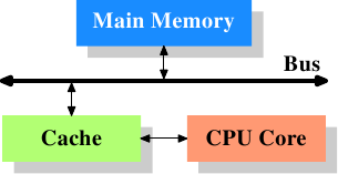
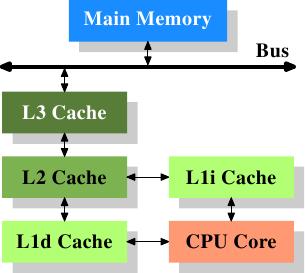
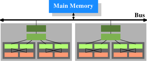
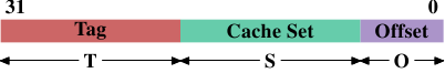
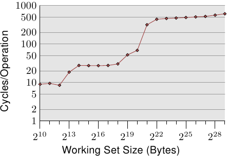

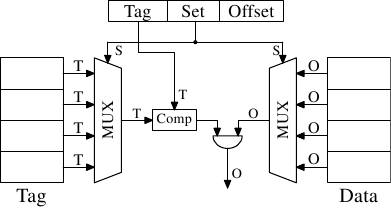
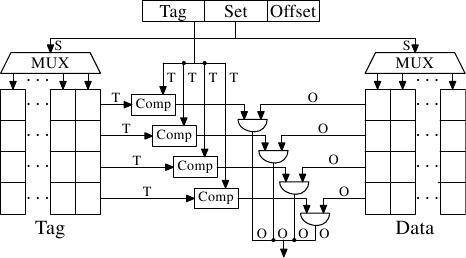
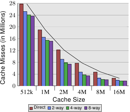
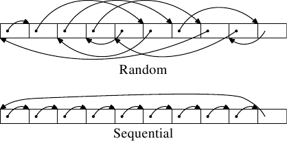
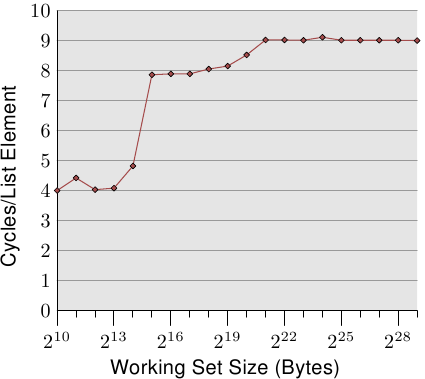
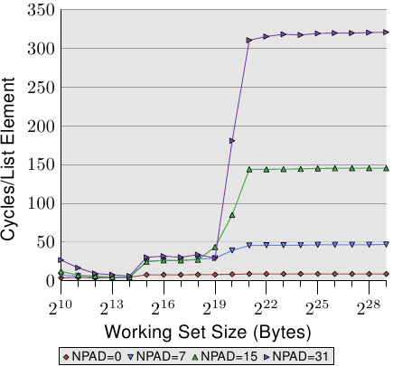
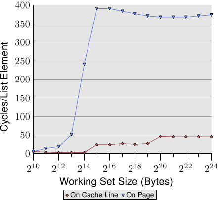
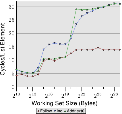
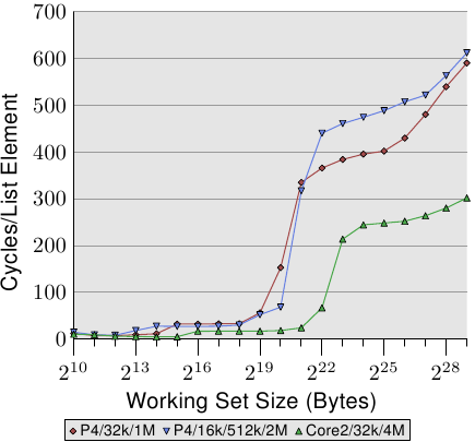
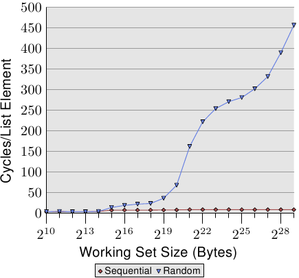
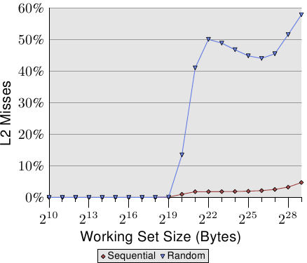
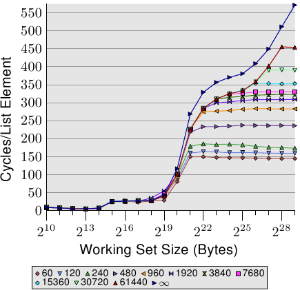
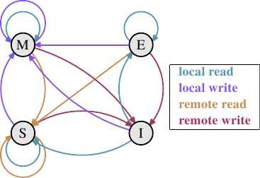
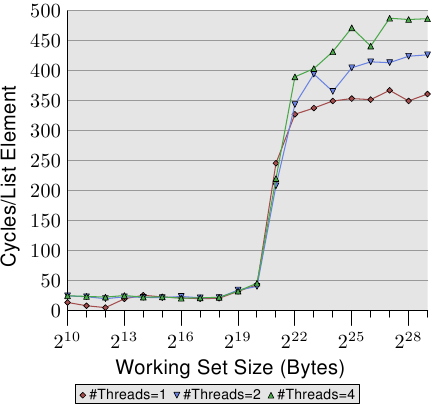
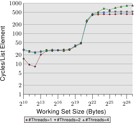
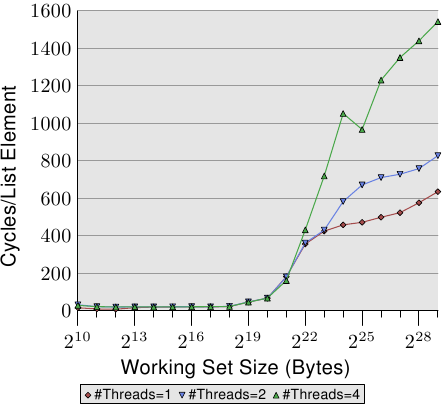
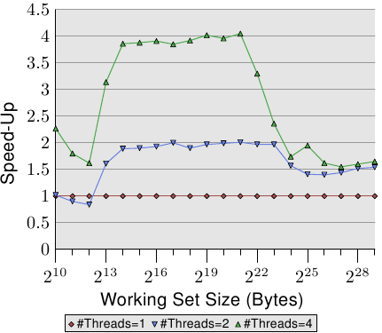
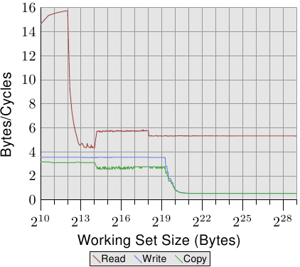

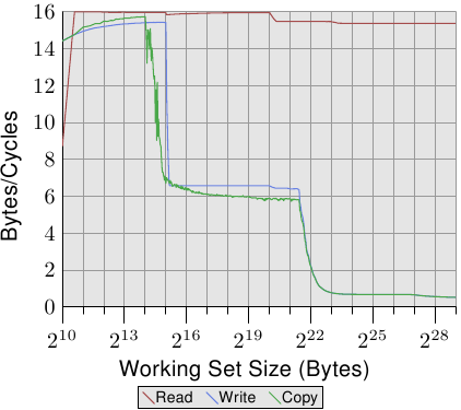


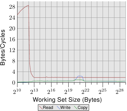
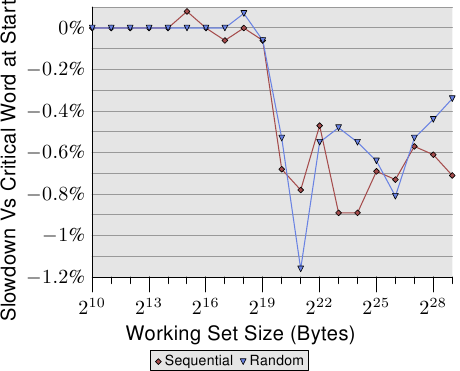
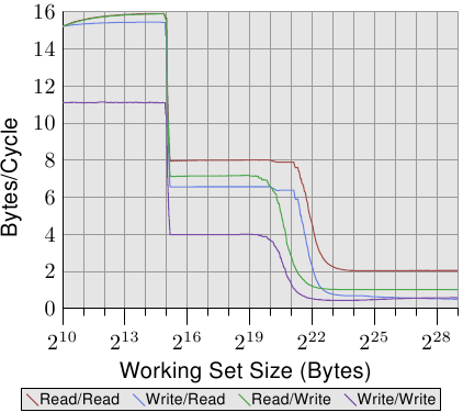
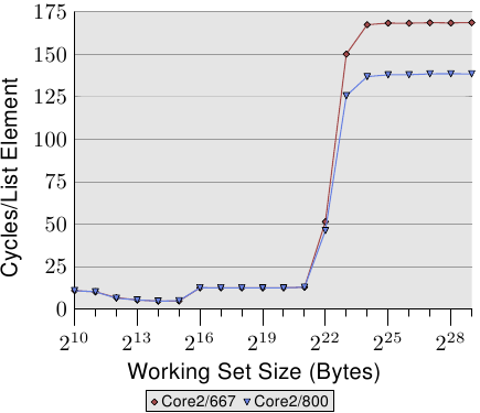
Part 3
[ Editor's note: this the third installment of Ulrich Drepper's "What every programmer should know about memory" document; this section talks about virtual memory, and TLB performance in particular. Those who have not read part 1 and part 2 may wish to do so now. As always, please send typo reports and the like to lwn@lwn.net rather than posting them as comments here.]
4 Virtual MemoryThe virtual memory subsystem of a processor implements the virtual address spaces provided to each process. This makes each process think it is alone in the system. The list of advantages of virtual memory are described in detail elsewhere so they will not be repeated here. Instead this section concentrates on the actual implementation details of the virtual memory subsystem and the associated costs. |
译者信息
[编辑注:本文是Ulrich Drepper的“每个程序员应该了解的内存方面的知识”文章的第三部分;这一部分谈论了虚拟内存,特别是TLB性能。没有阅读第1部分和第2部分的人可能现在就想读一读了。和往常一样,请将排字错误报告之类发送到lwn@lwn.net,而不要发送到这里的评论。] 4 虚拟内存 处理器的虚拟内存子系统为每个进程实现了虚拟地址空间。这让每个进程认为它在系统中是独立的。虚拟内存的优点列表别的地方描述的非常详细,所以这里就不重复了。本节集中在虚拟内存的实际的实现细节,和相关的成本。 |
|
A virtual address space is implemented by the Memory Management Unit (MMU) of the CPU. The OS has to fill out the page table data structures, but most CPUs do the rest of the work themselves. This is actually a pretty complicated mechanism; the best way to understand it is to introduce the data structures used to describe the virtual address space. The input to the address translation performed by the MMU is a virtual address. There are usually few—if any—restrictions on its value. Virtual addresses are 32-bit values on 32-bit systems, and 64-bit values on 64-bit systems. On some systems, for instance x86 and x86-64, the addresses used actually involve another level of indirection: these architectures use segments which simply cause an offset to be added to every logical address. We can ignore this part of address generation, it is trivial and not something that programmers have to care about with respect to performance of memory handling. {Segment limits on x86 are performance-relevant but that is another story.} |
译者信息
虚拟地址空间是由CPU的内存管理单元(MMU)实现的。OS必须填充页表数据结构,但大多数CPU自己做了剩下的工作。这事实上是一个相当复杂的机制;最好的理解它的方法是引入数据结构来描述虚拟地址空间。 由MMU进行地址翻译的输入地址是虚拟地址。通常对它的值很少有限制 — 假设还有一点的话。 虚拟地址在32位系统中是32位的数值,在64位系统中是64位的数值。在一些系统,例如x86和x86-64,使用的地址实际上包含了另一个层次的间接寻址:这些结构使用分段,这些分段只是简单的给每个逻辑地址加上位移。我们可以忽略这一部分的地址产生,它不重要,不是程序员非常关心的内存处理性能方面的东西。{x86的分段限制是与性能相关的,但那是另一回事了} |
4.1 Simplest Address TranslationThe interesting part is the translation of the virtual address to a physical address. The MMU can remap addresses on a page-by-page basis. Just as when addressing cache lines, the virtual address is split into distinct parts. These parts are used to index into various tables which are used in the construction of the final physical address. For the simplest model we have only one level of tables.
Figure 4.1 shows how the different parts of the virtual address are used. A top part is used to select an entry in a Page Directory; each entry in that directory can be individually set by the OS. The page directory entry determines the address of a physical memory page; more than one entry in the page directory can point to the same physical address. The complete physical address of the memory cell is determined by combining the page address from the page directory with the low bits from the virtual address. The page directory entry also contains some additional information about the page such as access permissions. |
译者信息
4.1 最简单的地址转换有趣的地方在于由虚拟地址到物理地址的转换。MMU可以在逐页的基础上重新映射地址。就像地址缓存排列的时候,虚拟地址被分割为不同的部分。这些部分被用来做多个表的索引,而这些表是被用来创建最终物理地址用的。最简单的模型是只有一级表。
图 4.1 显示了虚拟地址的不同部分是如何使用的。高字节部分是用来选择一个页目录的条目;那个目录中的每个地址可以被OS分别设置。页目录条目决定了物理内存页的地址;页面中可以有不止一个条目指向同样的物理地址。完整的内存物理地址是由页目录获得的页地址和虚拟地址低字节部分合并起来决定的。页目录条目还包含一些附加的页面信息,如访问权限。 |
|
The data structure for the page directory is stored in memory. The OS has to allocate contiguous physical memory and store the base address of this memory region in a special register. The appropriate bits of the virtual address are then used as an index into the page directory, which is actually an array of directory entries. For a concrete example, this is the layout used for 4MB pages on x86 machines. The Offset part of the virtual address is 22 bits in size, enough to address every byte in a 4MB page. The remaining 10 bits of the virtual address select one of the 1024 entries in the page directory. Each entry contains a 10 bit base address of a 4MB page which is combined with the offset to form a complete 32 bit address. |
译者信息
页目录的数据结构存储在内存中。OS必须分配连续的物理内存,并将这个地址范围的基地址存入一个特殊的寄存器。然后虚拟地址的适当的位被用来作为页目录的索引,这个页目录事实上是目录条目的列表。 作为一个具体的例子,这是 x86机器4MB分页设计。虚拟地址的位移部分是22位大小,足以定位一个4M页内的每一个字节。虚拟地址中剩下的10位指定页目录中1024个条目的一个。每个条目包括一个10位的4M页内的基地址,它与位移结合起来形成了一个完整的32位地址。 |
4.2 Multi-Level Page Tables4MB pages are not the norm, they would waste a lot of memory since many operations an OS has to perform require alignment to memory pages. With 4kB pages (the norm on 32-bit machines and, still, often on 64-bit machines), the Offset part of the virtual address is only 12 bits in size. This leaves 20 bits as the selector of the page directory. A table with 220 entries is not practical. Even if each entry would be only 4 bytes the table would be 4MB in size. With each process potentially having its own distinct page directory much of the physical memory of the system would be tied up for these page directories. The solution is to use multiple levels of page tables. These can then represent a sparse huge page directory where regions which are not actually used do not require allocated memory. The representation is therefore much more compact, making it possible to have the page tables for many processes in memory without impacting performance too much. |
译者信息
4.2 多级页表4MB的页不是规范,它们会浪费很多内存,因为OS需要执行的许多操作需要内存页的队列。对于4kB的页(32位机器的规范,甚至通常是64位机器的规范),虚拟地址的位移部分只有12位大小。这留下了20位作为页目录的指针。具有220个条目的表是不实际的。即使每个条目只要4比特,这个表也要4MB大小。由于每个进程可能具有其唯一的页目录,因为这些页目录许多系统中物理内存被绑定起来。 解决办法是用多级页表。然后这些就能表示一个稀疏的大的页目录,目录中一些实际不用的区域不需要分配内存。因此这种表示更紧凑,使它可能为内存中的很多进程使用页表而并不太影响性能。. |
|
Today the most complicated page table structures comprise four levels. Figure 4.2 shows the schematics of such an implementation.
The virtual address is, in this example, split into at least five parts. Four of these parts are indexes into the various directories. The level 4 directory is referenced using a special-purpose register in the CPU. The content of the level 4 to level 2 directories is a reference to next lower level directory. If a directory entry is marked empty it obviously need not point to any lower directory. This way the page table tree can be sparse and compact. The entries of the level 1 directory are, just like in Figure 4.1, partial physical addresses, plus auxiliary data like access permissions. |
译者信息
今天最复杂的页表结构由四级构成。图4.2显示了这样一个实现的原理图。
在这个例子中,虚拟地址被至少分为五个部分。其中四个部分是不同的目录的索引。被引用的第4级目录使用CPU中一个特殊目的的寄存器。第4级到第2级目录的内容是对次低一级目录的引用。如果一个目录条目标识为空,显然就是不需要指向任何低一级的目录。这样页表树就能稀疏和紧凑。正如图4.1,第1级目录的条目是一部分物理地址,加上像访问权限的辅助数据。 |
|
To determine the physical address corresponding to a virtual address the processor first determines the address of the highest level directory. This address is usually stored in a register. Then the CPU takes the index part of the virtual address corresponding to this directory and uses that index to pick the appropriate entry. This entry is the address of the next directory, which is indexed using the next part of the virtual address. This process continues until it reaches the level 1 directory, at which point the value of the directory entry is the high part of the physical address. The physical address is completed by adding the page offset bits from the virtual address. This process is called page tree walking. Some processors (like x86 and x86-64) perform this operation in hardware, others need assistance from the OS. |
译者信息为了决定相对于虚拟地址的物理地址,处理器先决定最高级目录的地址。这个地址一般保存在一个寄存器。然后CPU取出虚拟地址中相对于这个目录的索引部分,并用那个索引选择合适的条目。这个条目是下一级目录的地址,它由虚拟地址的下一部分索引。处理器继续直到它到达第1级目录,那里那个目录条目的值就是物理地址的高字节部分。物理地址在加上虚拟地址中的页面位移之后就完整了。这个过程称为页面树遍历。一些处理器(像x86和x86-64)在硬件中执行这个操作,其他的需要OS的协助。 |
|
Each process running on the system might need its own page table tree. It is possible to partially share trees but this is rather the exception. It is therefore good for performance and scalability if the memory needed by the page table trees is as small as possible. The ideal case for this is to place the used memory close together in the virtual address space; the actual physical addresses used do not matter. A small program might get by with using just one directory at each of levels 2, 3, and 4 and a few level 1 directories. On x86-64 with 4kB pages and 512 entries per directory this allows the addressing of 2MB with a total of 4 directories (one for each level). 1GB of contiguous memory can be addressed with one directory for levels 2 to 4 and 512 directories for level 1. Assuming all memory can be allocated contiguously is too simplistic, though. For flexibility reasons the stack and the heap area of a process are, in most cases, allocated at pretty much opposite ends of the address space. This allows either area to grow as much as possible if needed. This means that there are most likely two level 2 directories needed and correspondingly more lower level directories. |
译者信息
系统中运行的每个进程可能需要自己的页表树。有部分共享树的可能,但是这相当例外。因此如果页表树需要的内存尽可能小的话将对性能与可扩展性有利。理想的情况是将使用的内存紧靠着放在虚拟地址空间;但实际使用的物理地址不影响。一个小程序可能只需要第2,3,4级的一个目录和少许第1级目录就能应付过去。在一个采用4kB页面和每个目录512条目的x86-64机器上,这允许用4级目录对2MB定位(每一级一个)。1GB连续的内存可以被第2到第4级的一个目录和第1级的512个目录定位。 但是,假设所有内存可以被连续分配是太简单了。由于复杂的原因,大多数情况下,一个进程的栈与堆的区域是被分配在地址空间中非常相反的两端。这样使得任一个区域可以根据需要尽可能的增长。这意味着最有可能需要两个第2级目录和相应的更多的低一级的目录。 |
|
But even this does not always match current practice. For security reasons the various parts of an executable (code, data, heap, stack, DSOs, aka shared libraries) are mapped at randomized addresses [nonselsec]. The randomization extends to the relative position of the various parts; that implies that the various memory regions in use in a process are widespread throughout the virtual address space. By applying some limits to the number of bits of the address which are randomized the range can be restricted, but it certainly, in most cases, will not allow a process to run with just one or two directories for levels 2 and 3. If performance is really much more important than security, randomization can be turned off. The OS will then usually at least load all DSOs contiguously in virtual memory. |
译者信息
但即使这也不常常匹配现在的实际。由于安全的原因,一个可运行的(代码,数据,堆,栈,动态共享对象,aka共享库)不同的部分被映射到随机的地址[未选中的]。随机化延伸到不同部分的相对位置;那意味着一个进程使用的不同的内存范围,遍布于虚拟地址空间。通过对随机的地址位数采用一些限定,范围可以被限制,但在大多数情况下,这当然不会让一个进程只用一到两个第2和第3级目录运行。 如果性能真的远比安全重要,随机化可以被关闭。OS然后通常是在虚拟内存中至少连续的装载所有的动态共享对象(DSO)。 |
4.3 Optimizing Page Table AccessAll the data structures for the page tables are kept in the main memory; this is where the OS constructs and updates the tables. Upon creation of a process or a change of a page table the CPU is notified. The page tables are used to resolve every virtual address into a physical address using the page table walk described above. More to the point: at least one directory for each level is used in the process of resolving a virtual address. This requires up to four memory accesses (for a single access by the running process) which is slow. It is possible to treat these directory table entries as normal data and cache them in L1d, L2, etc., but this would still be far too slow. |
译者信息
4.3 优化页表访问页表的所有数据结构都保存在主存中;在那里OS建造和更新这些表。当一个进程创建或者一个页表变化,CPU将被通知。页表被用来解决每个虚拟地址到物理地址的转换,用上面描述的页表遍历方式。更多有关于此:至少每一级有一个目录被用于处理虚拟地址的过程。这需要至多四次内存访问(对一个运行中的进程的单次访问来说),这很慢。有可能像普通数据一样处理这些目录表条目,并将他们缓存在L1d,L2等等,但这仍然非常慢。 |
|
From the earliest days of virtual memory, CPU designers have used a different optimization. A simple computation can show that only keeping the directory table entries in the L1d and higher cache would lead to horrible performance. Each absolute address computation would require a number of L1d accesses corresponding to the page table depth. These accesses cannot be parallelized since they depend on the previous lookup's result. This alone would, on a machine with four page table levels, require at the very least 12 cycles. Add to that the probability of an L1d miss and the result is nothing the instruction pipeline can hide. The additional L1d accesses also steal precious bandwidth to the cache. |
译者信息从虚拟内存的早期阶段开始,CPU的设计者采用了一种不同的优化。简单的计算显示,只有将目录表条目保存在L1d和更高级的缓存,才会导致可怕的性能问题。每个绝对地址的计算,都需要相对于页表深度的大量的L1d访问。这些访问不能并行,因为它们依赖于前面查询的结果。在一个四级页表的机器上,这种单线性将 至少至少需要12次循环。再加上L1d的非命中的可能性,结果是指令流水线没有什么能隐藏的。额外的L1d访问也消耗了珍贵的缓存带宽。 |
|
So, instead of just caching the directory table entries, the complete computation of the address of the physical page is cached. For the same reason that code and data caches work, such a cached address computation is effective. Since the page offset part of the virtual address does not play any part in the computation of the physical page address, only the rest of the virtual address is used as the tag for the cache. Depending on the page size this means hundreds or thousands of instructions or data objects share the same tag and therefore same physical address prefix. The cache into which the computed values are stored is called the Translation Look-Aside Buffer (TLB). It is usually a small cache since it has to be extremely fast. Modern CPUs provide multi-level TLB caches, just as for the other caches; the higher-level caches are larger and slower. The small size of the L1TLB is often made up for by making the cache fully associative, with an LRU eviction policy. Recently, this cache has been growing in size and, in the process, was changed to be set associative. As a result, it might not be the oldest entry which gets evicted and replaced whenever a new entry has to be added. |
译者信息
所以,替代于只是缓存目录表条目,物理页地址的完整的计算结果被缓存了。因为同样的原因,代码和数据缓存也工作起来,这样的地址计算结果的缓存是高效的。由于虚拟地址的页面位移部分在物理页地址的计算中不起任何作用,只有虚拟地址的剩余部分被用作缓存的标签。根据页面大小这意味着成百上千的指令或数据对象共享同一个标签,因此也共享同一个物理地址前缀。 保存计算数值的缓存叫做旁路转换缓存(TLB)。因为它必须非常的快,通常这是一个小的缓存。现代CPU像其它缓存一样,提供了多级TLB缓存;越高级的缓存越大越慢。小号的L1级TLB通常被用来做全相联映像缓存,采用LRU回收策略。最近这种缓存大小变大了,而且在处理器中变得集相联。其结果之一就是,当一个新的条目必须被添加的时候,可能不是最久的条目被回收于替换了。 |
|
As noted above, the tag used to access the TLB is a part of the virtual address. If the tag has a match in the cache, the final physical address is computed by adding the page offset from the virtual address to the cached value. This is a very fast process; it has to be since the physical address must be available for every instruction using absolute addresses and, in some cases, for L2 look-ups which use the physical address as the key. If the TLB lookup misses the processor has to perform a page table walk; this can be quite costly. Prefetching code or data through software or hardware could implicitly prefetch entries for the TLB if the address is on another page. This cannot be allowed for hardware prefetching because the hardware could initiate page table walks that are invalid. Programmers therefore cannot rely on hardware prefetching to prefetch TLB entries. It has to be done explicitly using prefetch instructions. TLBs, just like data and instruction caches, can appear in multiple levels. Just as for the data cache, the TLB usually appears in two flavors: an instruction TLB (ITLB) and a data TLB (DTLB). Higher-level TLBs such as the L2TLB are usually unified, as is the case with the other caches. |
译者信息
正如上面提到的,用来访问TLB的标签是虚拟地址的一个部分。如果标签在缓存中有匹配,最终的物理地址将被计算出来,通过将来自虚拟地址的页面位移地址加到缓存值的方式。这是一个非常快的过程;也必须这样,因为每条使用绝对地址的指令都需要物理地址,还有在一些情况下,因为使用物理地址作为关键字的L2查找。如果TLB查询未命中,处理器就必须执行一次页表遍历;这可能代价非常大。 通过软件或硬件预取代码或数据,会在地址位于另一页面时,暗中预取TLB的条目。硬件预取不可能允许这样,因为硬件会初始化非法的页面表遍历。因此程序员不能依赖硬件预取机制来预取TLB条目。它必须使用预取指令明确的完成。就像数据和指令缓存,TLB可以表现为多个等级。正如数据缓存,TLB通常表现为两种形式:指令TLB(ITLB)和数据TLB(DTLB)。高级的TLB像L2TLB通常是统一的,就像其他的缓存情形一样。 |
|
4.3.1 Caveats Of Using A TLB The TLB is a processor-core global resource. All threads and processes executed on the processor core use the same TLB. Since the translation of virtual to physical addresses depends on which page table tree is installed, the CPU cannot blindly reuse the cached entries if the page table is changed. Each process has a different page table tree (but not the threads in the same process) as does the kernel and the VMM (hypervisor) if present. It is also possible that the address space layout of a process changes. There are two ways to deal with this problem:
In the first case the TLB is flushed whenever a context switch is performed. Since, in most OSes, a switch from one thread/process to another one requires executing some kernel code, TLB flushes are restricted to entering and leaving the kernel address space. On virtualized systems it also happens when the kernel has to call the VMM and on the way back. If the kernel and/or VMM does not have to use virtual addresses, or can reuse the same virtual addresses as the process or kernel which made the system/VMM call, the TLB only has to be flushed if, upon leaving the kernel or VMM, the processor resumes execution of a different process or kernel. |
译者信息
4.3.1 使用TLB的注意事项 TLB是以处理器为核心的全局资源。所有运行于处理器的线程与进程使用同一个TLB。由于虚拟到物理地址的转换依赖于安装的是哪一种页表树,如果页表变化了,CPU不能盲目的重复使用缓存的条目。每个进程有一个不同的页表树(不算在同一个进程中的线程),内核与内存管理器VMM(管理程序)也一样,如果存在的话。也有可能一个进程的地址空间布局发生变化。有两种解决这个问题的办法:
第一种情况,只要执行一个上下文切换TLB就被刷新。因为大多数OS中,从一个线程/进程到另一个的切换需要执行一些核心代码,TLB刷新被限制进入或离开核心地址空间。在虚拟化的系统中,当内核必须调用内存管理器VMM和返回的时候,这也会发生。如果内核和/或内存管理器没有使用虚拟地址,或者当进程或内核调用系统/内存管理器时,能重复使用同一个虚拟地址,TLB必须被刷新。当离开内核或内存管理器时,处理器继续执行一个不同的进程或内核。 |
|
Flushing the TLB is effective but expensive. When executing a system call, for instance, the kernel code might be restricted to a few thousand instructions which touch, perhaps, a handful of new pages (or one huge page, as is the case for Linux on some architectures). This work would replace only as many TLB entries as pages are touched. For Intel's Core2 architecture with its 128 ITLB and 256 DTLB entries, a full flush would mean that more than 100 and 200 entries (respectively) would be flushed unnecessarily. When the system call returns to the same process, all those flushed TLB entries could be used again, but they will be gone. The same is true for often-used code in the kernel or VMM. On each entry into the kernel the TLB has to be filled from scratch even though the page tables for the kernel and VMM usually do not change and, therefore, TLB entries could, in theory, be preserved for a very long time. This also explains why the TLB caches in today's processors are not bigger: programs most likely will not run long enough to fill all these entries. |
译者信息刷新TLB高效但昂贵。例如,当执行一个系统调用,触及的内核代码可能仅限于几千条指令,或许少许新页面(或一个大的页面,像某些结构的Linux的就是这样)。这个工作将替换触及页面的所有TLB条目。对Intel带128ITLB和256DTLB条目的Core2架构,完全的刷新意味着多于100和200条目(分别的)将被不必要的刷新。当系统调用返回同一个进程,所有那些被刷新的TLB条目可能被再次用到,但它们没有了。内核或内存管理器常用的代码也一样。每条进入内核的条目上,TLB必须擦去再装,即使内核与内存管理器的页表通常不会改变。因此理论上说,TLB条目可以被保持一个很长时间。这也解释了为什么现在处理器中的TLB缓存都不大:程序很有可能不会执行时间长到装满所有这些条目。 |
|
This fact, of course, did not escape the CPU architects. One possibility to optimize the cache flushes is to individually invalidate TLB entries. For instance, if the kernel code and data falls into a specific address range, only the pages falling into this address range have to evicted from the TLB. This only requires comparing tags and, therefore, is not very expensive. This method is also useful in case a part of the address space is changed, for instance, through a call tomunmap. A much better solution is to extend the tag used for the TLB access. If, in addition to the part of the virtual address, a unique identifier for each page table tree (i.e., a process's address space) is added, the TLB does not have to be completely flushed at all. The kernel, VMM, and the individual processes all can have unique identifiers. The only issue with this scheme is that the number of bits available for the TLB tag is severely limited, while the number of address spaces is not. This means some identifier reuse is necessary. When this happens the TLB has to be partially flushed (if this is possible). All entries with the reused identifier must be flushed but this is, hopefully, a much smaller set. |
译者信息
当然事实逃脱不了CPU的结构。对缓存刷新优化的一个可能的方法是单独的使TLB条目失效。例如,如果内核代码与数据落于一个特定的地址范围,只有落入这个地址范围的页面必须被清除出TLB。这只需要比较标签,因此不是很昂贵。在部分地址空间改变的场合,例如对去除内存页的一次调用,这个方法也是有用的, 更好的解决方法是为TLB访问扩展标签。如果除了虚拟地址的一部分之外,一个唯一的对应每个页表树的标识(如一个进程的地址空间)被添加,TLB将根本不需要完全刷新。内核,内存管理程序,和独立的进程都可以有唯一的标识。这种场景唯一的问题在于,TLB标签可以获得的位数异常有限,但是地址空间的位数却不是。这意味着一些标识的再利用是有必要的。这种情况发生时TLB必须部分刷新(如果可能的话)。所有带有再利用标识的条目必须被刷新,但是希望这是一个非常小的集合。 |
|
This extended TLB tagging is of general advantage when multiple processes are running on the system. If the memory use (and hence TLB entry use) of each of the runnable processes is limited, there is a good chance the most recently used TLB entries for a process are still in the TLB when it gets scheduled again. But there are two additional advantages:
|
译者信息
当多个进程运行在系统中时,这种扩展的TLB标签具有一般优势。如果每个可运行进程对内存的使用(因此TLB条目的使用)做限制,进程最近使用的TLB条目,当其再次列入计划时,有很大机会仍然在TLB。但还有两个额外的优势:
|
| Some processors have, for some time, implemented these extended tags. AMD introduced a 1-bit tag extension with the Pacifica virtualization extensions. This 1-bit Address Space ID (ASID) is, in the context of virtualization, used to distinguish the VMM's address space from that of the guest domains. This allows the OS to avoid flushing the guest's TLB entries every time the VMM is entered (for instance, to handle a page fault) or the VMM's TLB entries when control returns to the guest. The architecture will allow the use of more bits in the future. Other mainstream processors will likely follow suit and support this feature. | 译者信息有些处理器在一些时候实现了这些扩展标签。AMD给帕西菲卡(Pacifica)虚拟化扩展引入了一个1位的扩展标签。在虚拟化的上下文中,这个1位的地址空间ID(ASID)被用来从客户域区别出内存管理程序的地址空间。这使得OS能够避免在每次进入内存管理程序的时候(例如为了处理一个页面错误)刷新客户的TLB条目,或者当控制回到客户时刷新内存管理程序的TLB条目。这个架构未来会允许使用更多的位。其它主流处理器很可能会随之适应并支持这个功能。 |
|
4.3.2 Influencing TLB Performance There are a couple of factors which influence TLB performance. The first is the size of the pages. Obviously, the larger a page is, the more instructions or data objects will fit into it. So a larger page size reduces the overall number of address translations which are needed, meaning that fewer entries in the TLB cache are needed. Most architectures allow the use of multiple different page sizes; some sizes can be used concurrently. For instance, the x86/x86-64 processors have a normal page size of 4kB but they can also use 4MB and 2MB pages respectively. IA-64 and PowerPC allow sizes like 64kB as the base page size. The use of large page sizes brings some problems with it, though. The memory regions used for the large pages must be contiguous in physical memory. If the unit size for the administration of physical memory is raised to the size of the virtual memory pages, the amount of wasted memory will grow. All kinds of memory operations (like loading executables) require alignment to page boundaries. This means, on average, that each mapping wastes half the page size in physical memory for each mapping. This waste can easily add up; it thus puts an upper limit on the reasonable unit size for physical memory allocation. |
译者信息
4.3.2 影响TLB性能 有一些因素会影响TLB性能。第一个是页面的大小。显然页面越大,装进去的指令或数据对象就越多。所以较大的页面大小减少了所需的地址转换总次数,即需要更少的TLB缓存条目。大多数架构允许使用多个不同的页面尺寸;一些尺寸可以并存使用。例如,x86/x86-64处理器有一个普通的4kB的页面尺寸,但它们也可以分别用4MB和2MB页面。IA-64 和 PowerPC允许如64kB的尺寸作为基本的页面尺寸。 然而,大页面尺寸的使用也随之带来了一些问题。用作大页面的内存范围必须是在物理内存中连续的。如果物理内存管理的单元大小升至虚拟内存页面的大小,浪费的内存数量将会增长。各种内存操作(如加载可执行文件)需要页面边界对齐。这意味着平均每次映射浪费了物理内存中页面大小的一半。这种浪费很容易累加;因此它给物理内存分配的合理单元大小划定了一个上限。 |
|
It is certainly not practical to increase the unit size to 2MB to accommodate large pages on x86-64. This is just too large a size. But this in turn means that each large page has to be comprised of many smaller pages. And these small pages have to be contiguous in physical memory. Allocating 2MB of contiguous physical memory with a unit page size of 4kB can be challenging. It requires finding a free area with 512 contiguous pages. This can be extremely difficult (or impossible) after the system runs for a while and physical memory becomes fragmented. On Linux it is therefore necessary to pre-allocate these big pages at system start time using the specialhugetlbfsfilesystem. A fixed number of physical pages are reserved for exclusive use as big virtual pages. This ties down resources which might not always be used. It also is a limited pool; increasing it normally means restarting the system. Still, huge pages are the way to go in situations where performance is a premium, resources are plenty, and cumbersome setup is not a big deterrent. Database servers are an example. |
译者信息
在x86-64结构中增加单元大小到2MB来适应大页面当然是不实际的。这是一个太大的尺寸。但这转而意味着每个大页面必须由许多小一些的页面组成。这些小页面必须在物理内存中连续。以4kB单元页面大小分配2MB连续的物理内存具有挑战性。它需要找到有512个连续页面的空闲区域。在系统运行一段时间并且物理内存开始碎片化以后,这可能极为困难(或者不可能) 因此在Linux中有必要在系统启动的时候,用特别的Huge TLBfs文件系统,预分配这些大页面。一个固定数目的物理页面被保留,以单独用作大的虚拟页面。这使可能不会经常用到的资源捆绑留下来。它也是一个有限的池;增大它一般意味着要重启系统。尽管如此,大页面是进入某些局面的方法,在这些局面中性能具有保险性,资源丰富,而且麻烦的安装不会成为大的妨碍。数据库服务器就是一个例子。 |
|
Increasing the minimum virtual page size (as opposed to optional big pages) has its problems, too. Memory mapping operations (loading applications, for example) must conform to these page sizes. No smaller mappings are possible. The location of the various parts of an executable have, for most architectures, a fixed relationship. If the page size is increased beyond what has been taken into account when the executable or DSO was built, the load operation cannot be performed. It is important to keep this limitation in mind. Figure 4.3 shows how the alignment requirements of an ELF binary can be determined. It is encoded in the ELF program header. $ eu-readelf -l /bin/ls Program Headers: Type Offset VirtAddr PhysAddr FileSiz MemSiz Flg Align ... LOAD 0x000000 0x0000000000400000 0x0000000000400000 0x0132ac 0x0132ac R E 0x200000 LOAD 0x0132b0 0x00000000006132b0 0x00000000006132b0 0x001a71 0x001a71 RW 0x200000 ... Figure 4.3: ELF Program Header Indicating Alignment Requirements In this example, an x86-64 binary, the value is 0x200000 = 2,097,152 = 2MB which corresponds to the maximum page size supported by the processor. |
译者信息
增大最小的虚拟页面大小(正如选择大页面的相反面)也有它的问题。内存映射操作(例如加载应用)必须确认这些页面大小。不可能有更小的映射。对大多数架构来说,一个可执行程序的各个部分位置有一个固定的关系。如果页面大小增加到超过了可执行程序或DSO(Dynamic Shared Object)创建时考虑的大小,加载操作将无法执行。脑海里记得这个限制很重要。图4.3显示了一个ELF二进制的对齐需求是如何决定的。它编码在ELF程序头部。 $ eu-readelf -l /bin/ls Program Headers: Type Offset VirtAddr PhysAddr FileSiz MemSiz Flg Align ... LOAD 0x000000 0x0000000000400000 0x0000000000400000 0x0132ac 0x0132ac R E 0x200000 LOAD 0x0132b0 0x00000000006132b0 0x00000000006132b0 0x001a71 0x001a71 RW 0x200000 ... Figure 4.3: ELF 程序头表明了对齐需求 在这个例子中,一个x86-64二进制,它的值为0x200000 = 2,097,152 = 2MB,符合处理器支持的最大页面尺寸。 |
|
There is a second effect of using larger page sizes: the number of levels of the page table tree is reduced. Since the part of the virtual address corresponding to the page offset increases, there are not that many bits left which need to be handled through page directories. This means that, in case of a TLB miss, the amount of work which has to be done is reduced. Beyond using large page sizes, it is possible to reduce the number of TLB entries needed by moving data which is used at the same time to fewer pages. This is similar to some optimizations for cache use we talked about above. Only now the alignment required is large. Given that the number of TLB entries is quite small this can be an important optimization. |
译者信息
使用较大内存尺寸有第二个影响:页表树的级数减少了。由于虚拟地址相对于页面位移的部分增加了,需要用来在页目录中使用的位,就没有剩下许多了。这意味着当一个TLB未命中时,需要做的工作数量减少了。 超出使用大页面大小,它有可能减少移动数据时需要同时使用的TLB条目数目,减少到数页。这与一些上面我们谈论的缓存使用的优化机制类似。只有现在对齐需求是巨大的。考虑到TLB条目数目如此小,这可能是一个重要的优化。 |
4.4 Impact Of VirtualizationVirtualization of OS images will become more and more prevalent; this means another layer of memory handling is added to the picture. Virtualization of processes (basically jails) or OS containers do not fall into this category since only one OS is involved. Technologies like Xen or KVM enable—with or without help from the processor—the execution of independent OS images. In these situations there is one piece of software alone which directly controls access to the physical memory.
In the case of Xen (see Figure 4.4) the Xen VMM is that piece of software. The VMM does not implement many of the other hardware controls itself, though. Unlike VMMs on other, earlier systems (and the first release of the Xen VMM) the hardware outside of memory and processors is controlled by the privileged Dom0 domain. Currently, this is basically the same kernel as the unprivileged DomU kernels and, as far as memory handling is concerned, they do not differ. Important here is that the VMM hands out physical memory to the Dom0 and DomU kernels which, themselves, then implement the usual memory handling as if they were running directly on a processor. |
译者信息
4.4 虚拟化的影响OS映像的虚拟化将变得越来越流行;这意味着另一个层次的内存处理被加入了想象。进程(基本的隔间)或者OS容器的虚拟化,因为只涉及一个OS而没有落入此分类。类似Xen或KVM的技术使OS映像能够独立运行 — 有或者没有处理器的协助。这些情形下,有一个单独的软件直接控制物理内存的访问。
对Xen来说(见图4.4),Xen VMM(Xen内存管理程序)就是那个软件。但是,VMM没有自己实现许多硬件的控制,不像其他早先的系统(包括Xen VMM的第一个版本)的VMM,内存以外的硬件和处理器由享有特权的Dom0域控制。现在,这基本上与没有特权的DomU内核一样,就内存处理方面而言,它们没有什么不同。这里重要的是,VMM自己分发物理内存给Dom0和DomU内核,然后就像他们是直接运行在一个处理器上一样,实现通常的内存处理 |
|
To implement the separation of the domains which is required for the virtualization to be complete, the memory handling in the Dom0 and DomU kernels does not have unrestricted access to physical memory. The VMM does not hand out memory by giving out individual physical pages and letting the guest OSes handle the addressing; this would not provide any protection against faulty or rogue guest domains. Instead, the VMM creates its own page table tree for each guest domain and hands out memory using these data structures. The good thing is that access to the administrative information of the page table tree can be controlled. If the code does not have appropriate privileges it cannot do anything. |
译者信息为了实现完成虚拟化所需的各个域之间的分隔,Dom0和DomU内核中的内存处理不具有无限制的物理内存访问权限。VMM不是通过分发独立的物理页并让客户OS处理地址的方式来分发内存;这不能提供对错误或欺诈客户域的防范。替代的,VMM为每一个客户域创建它自己的页表树,并且用这些数据结构分发内存。好处是对页表树管理信息的访问能得到控制。如果代码没有合适的特权,它不能做任何事。 |
|
This access control is exploited in the virtualization Xen provides, regardless of whether para- or hardware (aka full) virtualization is used. The guest domains construct their page table trees for each process in a way which is intentionally quite similar for para- and hardware virtualization. Whenever the guest OS modifies its page tables the VMM is invoked. The VMM then uses the updated information in the guest domain to update its own shadow page tables. These are the page tables which are actually used by the hardware. Obviously, this process is quite expensive: each modification of the page table tree requires an invocation of the VMM. While changes to the memory mapping are not cheap without virtualization they become even more expensive now. |
译者信息在虚拟化的Xen支持中,这种访问控制已被开发,不管使用的是参数的或硬件的(又名全)虚拟化。客户域以意图上与参数的和硬件的虚拟化极为相似的方法,给每个进程创建它们的页表树。每当客户OS修改了VMM调用的页表,VMM就会用客户域中更新的信息去更新自己的影子页表。这些是实际由硬件使用的页表。显然这个过程非常昂贵:每次对页表树的修改都需要VMM的一次调用。而没有虚拟化时内存映射的改变也不便宜,它们现在变得甚至更昂贵。 |
|
The additional costs can be really large, considering that the changes from the guest OS to the VMM and back themselves are already quite expensive. This is why the processors are starting to have additional functionality to avoid the creation of shadow page tables. This is good not only because of speed concerns but it also reduces memory consumption by the VMM. Intel has Extended Page Tables (EPTs) and AMD calls it Nested Page Tables (NPTs). Basically both technologies have the page tables of the guest OSes produce virtual physical addresses. These addresses must then be further translated, using the per-domain EPT/NPT trees, into actual physical addresses. This will allow memory handling at almost the speed of the no-virtualization case since most VMM entries for memory handling are removed. It also reduces the memory use of the VMM since now only one page table tree for each domain (as opposed to process) has to be maintained. |
译者信息考虑到从客户OS的变化到VMM以及返回,其本身已经相当昂贵,额外的代价可能真的很大。这就是为什么处理器开始具有避免创建影子页表的额外功能。这样很好不仅是因为速度的问题,而且它减少了VMM消耗的内存。Intel有扩展页表(EPTs),AMD称之为嵌套页表(NPTs)。基本上两种技术都具有客户OS的页表,来产生虚拟的物理地址。然后通过每个域一个EPT/NPT树的方式,这些地址会被进一步转换为真实的物理地址。这使得可以用几乎非虚拟化情境的速度进行内存处理,因为大多数用来内存处理的VMM条目被移走了。它也减少了VMM使用的内存,因为现在一个域(相对于进程)只有一个页表树需要维护。 |
|
The results of the additional address translation steps are also stored in the TLB. That means the TLB does not store the virtual physical address but, instead, the complete result of the lookup. It was already explained that AMD's Pacifica extension introduced the ASID to avoid TLB flushes on each entry. The number of bits for the ASID is one in the initial release of the processor extensions; this is just enough to differentiate VMM and guest OS. Intel has virtual processor IDs (VPIDs) which serve the same purpose, only there are more of them. But the VPID is fixed for each guest domain and therefore it cannot be used to mark separate processes and avoid TLB flushes at that level, too. |
译者信息额外的地址转换步骤的结果也存储于TLB。那意味着TLB不存储虚拟物理地址,而替代以完整的查询结果。已经解释过AMD的帕西菲卡扩展为了避免TLB刷新而给每个条目引入ASID。ASID的位数在最初版本的处理器扩展中是一位;这正好足够区分VMM和客户OS。Intel有服务同一个目的的虚拟处理器ID(VPIDs),它们只有更多位。但对每个客户域VPID是固定的,因此它不能标记单独的进程,也不能避免TLB在那个级别刷新。 |
|
The amount of work needed for each address space modification is one problem with virtualized OSes. There is another problem inherent in VMM-based virtualization, though: there is no way around having two layers of memory handling. But memory handling is hard (especially when taking complications like NUMA into account, see Section 5). The Xen approach of using a separate VMM makes optimal (or even good) handling hard since all the complications of a memory management implementation, including “trivial” things like discovery of memory regions, must be duplicated in the VMM. The OSes have fully-fledged and optimized implementations; one really wants to avoid duplicating them.
|
译者信息
对虚拟OS,每个地址空间的修改需要的工作量是一个问题。但是还有另一个内在的基于VMM虚拟化的问题:没有什么办法处理两层的内存。但内存处理很难(特别是考虑到像NUMA一样的复杂性,见第5部分)。Xen方法使用一个单独的VMM,这使最佳的(或最好的)处理变得困难,因为所有内存管理实现的复杂性,包括像发现内存范围之类“琐碎的”事情,必须被复制于VMM。OS有完全成熟的与最佳的实现;人们确实想避免复制它们。
|
| This is why carrying the VMM/Dom0 model to its conclusion is such an attractive alternative. Figure 4.5 shows how the KVM Linux kernel extensions try to solve the problem. There is no separate VMM running directly on the hardware and controlling all the guests; instead, a normal Linux kernel takes over this functionality. This means the complete and sophisticated memory handling functionality in the Linux kernel is used to manage the memory of the system. Guest domains run alongside the normal user-level processes in what the creators call “guest mode”. The virtualization functionality, para- or full virtualization, is controlled by another user-level process, the KVM VMM. This is just another process which happens to control a guest domain using the special KVM device the kernel implements. | 译者信息这就是为什么对VMM/Dom0模型的分析是这么有吸引力的一个选择。图4.5显示了KVM的Linux内核扩展如何尝试解决这个问题的。并没有直接运行在硬件之上且管理所有客户的单独的VMM,替代的,一个普通的Linux内核接管了这个功能。这意味着Linux内核中完整且复杂的内存管理功能,被用来管理系统的内存。客户域运行于普通的用户级进程,创建者称其为“客户模式”。虚拟化的功能,参数的或全虚拟化的,被另一个用户级进程KVM VMM控制。这也就是另一个进程用特别的内核实现的KVM设备,去恰巧控制一个客户域。 |
|
The benefit of this model over the separate VMM of the Xen model is that, even though there are still two memory handlers at work when guest OSes are used, there only needs to be one implementation, that in the Linux kernel. It is not necessary to duplicate the same functionality in another piece of code like the Xen VMM. This leads to less work, fewer bugs, and, perhaps, less friction where the two memory handlers touch since the memory handler in a Linux guest makes the same assumptions as the memory handler in the outer Linux kernel which runs on the bare hardware. Overall, programmers must be aware that, with virtualization used, the cost of memory operations is even higher than without virtualization. Any optimization which reduces this work will pay off even more in virtualized environments. Processor designers will, over time, reduce the difference more and more through technologies like EPT and NPT but it will never completely go away. |
译者信息
这个模型相较Xen独立的VMM模型好处在于,即使客户OS使用时,仍然有两个内存处理程序在工作,只需要在Linux内核里有一个实现。不需要像Xen VMM那样从另一段代码复制同样的功能。这带来更少的工作,更少的bug,或许还有更少的两个内存处理程序接触产生的摩擦,因为一个Linux客户的内存处理程序与运行于裸硬件之上的Linux内核的外部内存处理程序,做出了相同的假设。 总的来说,程序员必须清醒认识到,采用虚拟化时,内存操作的代价比没有虚拟化要高很多。任何减少这个工作的优化,将在虚拟化环境付出更多。随着时间的过去,处理器的设计者将通过像EPT和NPT技术越来越减少这个差距,但它永远都不会完全消失。 |
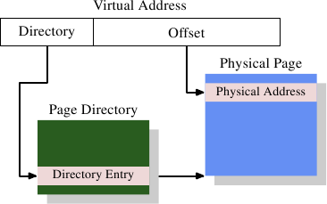


与大容量存储不同,