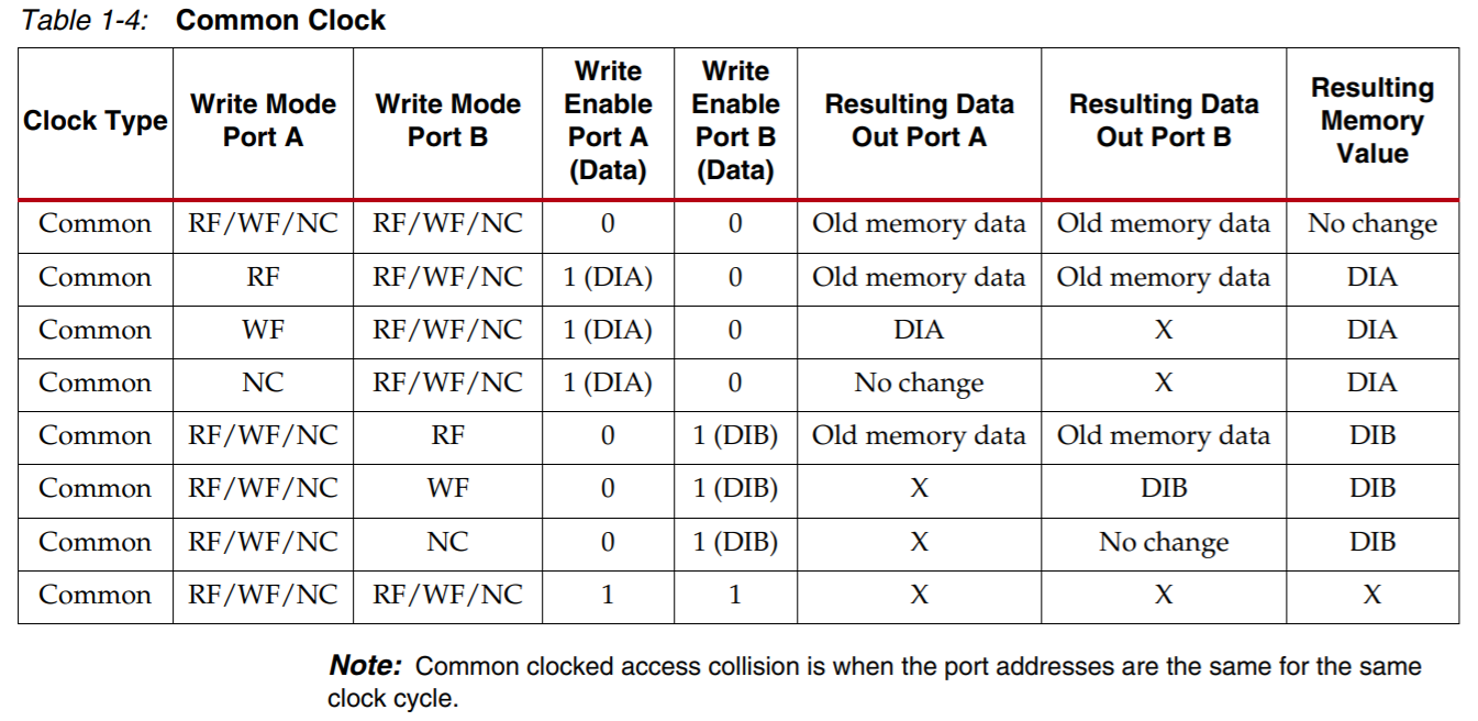
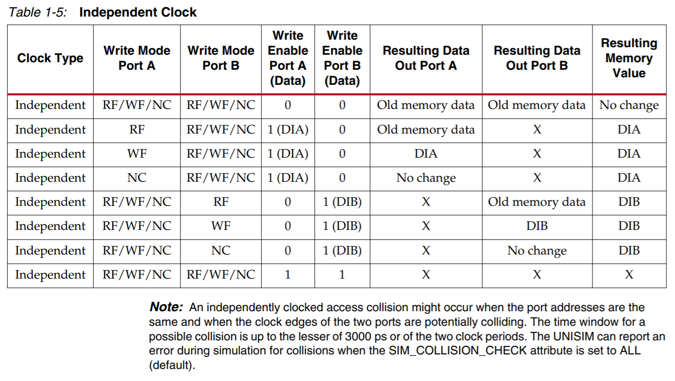
Conflict Avoidance
The 7 series FPGAs block RAM is a true dual-port RAM where both ports can access any memory location at any time. Address collisions can occur when accessing the same memory location from both ports. An address collision is when both block RAM ports access the same address location in the same clock cycle. There are two fundamental clock type setups, common clock and independent clock. Common (synchronous) clocks are driven by a common clock buffer driver. All other CLKA and CLKB connections are considered independent (asynchronous) clocks. If no address collisions are expected or possible (SDP configurations) to save power, the recommended write mode is NO_CHANGE. Using READ_FIRST mode has a 15% power penalty over NO_CHANGE and should only be used when necessary for functionality or address collision mitigation.
- When both ports are reading, the operations complete successfully.
- When both ports are writing different data, the memory location is written with non-deterministic data.
- When one port is writing and the other port is reading, the write is always successful but the resulting read memory value can vary. See Table 1-4 and Table 1-5. In Table 1-4 and Table 1-5:
- Write enable is active-High, 1 = Write, 0 = Read
- RF = READ_FIRST, WF = WRITE_FIRST, NC = NO_CHANGE
- X = Undeterministic value
- DIA = Port A data input
- DIB = Port B data input
Collision Behavior
The Block Memory Generator core supports Dual-port RAM implementations. Each port is equivalent and independent, yet they access the same memory space. In such an arrangement, is it possible to have data collisions. The ramifications of this behavior are described for both asynchronous and synchronous clocks.
Collisions and Asynchronous Clocks: General Guidelines
Using asynchronous clocks, when one port writes data to a memory location, the other port must not Read or Write that location for a specified amount of time. This clock-to-clock setup time is defined in the device data sheet, along with other block RAM switching characteristics.
Collisions and Synchronous Clocks: General Guidelines
Synchronous clocks cause a number of special case collision scenarios, described below.
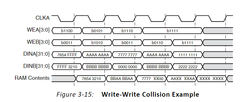
- Synchronous Write-Write Collisions: A Write-Write collision occurs if both ports attempt to Write to the same location in memory. The resulting contents of the memory location are unknown. Note that Write-Write collisions affect memory content, as opposed to Write-Read collisions which only affect data output.
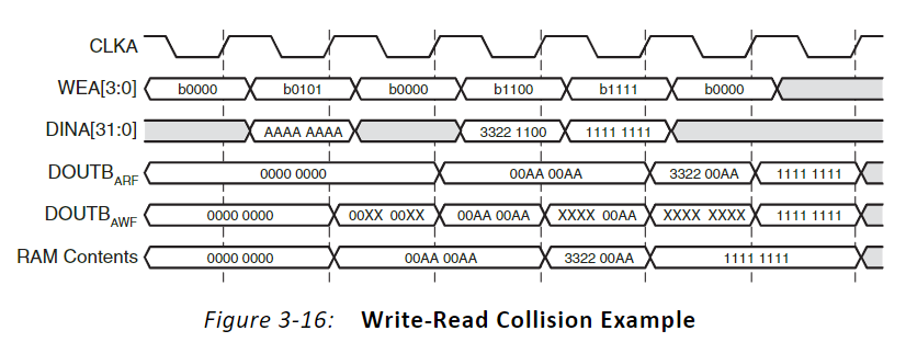
- Using Byte-Writes: When using byte-writes, memory contents are not corrupted when separate bytes are written in the same data word. RAM contents are corrupted only when both ports attempt to Write the same byte. Figure 3-15 illustrates this case. Assume addra = addrb = 0.
- Synchronous Write-Read Collisions: A synchronous Write-Read collision might occur if a port attempts to Write a memory location and the other port reads the same location. While memory contents are not corrupted in Write-Read collisions, the validity of the output data depends on the Write port operating mode.
- If the Write port is in READ_FIRST mode, the other port can reliably read the old memory contents.
- If the Write port is in WRITE_FIRST or NO_CHANGE mode, data on the output of the Read port is invalid.
- In the case of byte-writes, only updated bytes are invalid on the Read port output.
Figure 3-16 illustrates Write-Read collisions and the effects of byte-writes. doutb is shown for when port A is in WRITE_FIRST mode and READ_FIRST mode. Assume addra = addrb = 0, port B is always reading, and all memory locations are initialized to 0. The RAM contents are never corrupted in Write-Read collisions.