Introduction
The majority of image sensors in the consumer market use the MIPI CSI2 interface. The Mobile Industry Processor
Interface (MIPI) has become the interface standard for the majority of components in consumer mobile devices.
CSI2 (Camera Serial Interface 2) is the MIPI interface specification focused specifically on cameras. Because of
the high volume and cost optimized design of these image sensors, many embedded application designers are
interested in using these CSI2 image sensors. The challenge is that traditional ISPs (Image Signal Processors) do
not have a CSI2 interface. Many have a traditional CMOS bus for camera interfaces. ISPs with a parallel CMOS
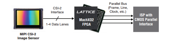
interface bus must use an external bridge to convert from CSI2 to parallel CMOS. The Lattice MIPI CSI2-to-CMOS
Parallel Sensor Bridge reference design performs this conversion in the ultra-low density MachXO2™-1200HC
FPGA.
Figure 1. CSI2 to CMOS Parallel Functional Block Diagram
Key Features
• Supports CSI2 high-speed differential signaling
– From one to four lanes, running at up to ~800 Mbps
– Supports 200 mV common mode voltage in High-Speed (HS) mode
• Provides parallel sensor output
– Output bus widths of 6 to 24 bits RAW, RGB and YUV
• Bridge device offered in space-saving 8x8mm 132-ball csBGA package. TQFP packages also available.
• Requires no external PROM
• Tested using the Sony IMX169 image sensor device on the Lattice CSI2 to Parallel Bridge Board and the HDR-
60 Base Board
– 1080p30 2-lane and 4-lane configurations can be demonstrated
• Parallel interface can be configured for 1.8V, 2.5V or 3.3V LVCMOS levels
• MachXO2 is available in commercial and industrial temperature grades