W25QXX系列芯片手册学习
概况
The W25Q128BV (8M-bit) Serial Flash memory provides a storage solution for systems with limited space, pins and power. The 25Q series offers flexibility and performance well beyond ordinary Serial Flash devices. They are ideal for code shadowing to RAM, executing code directly from Dual/Quad SPI (XIP) and storing voice, text and data. The device operates on a single 2.7V to 3.6V power supply with current consumption as low as 4mA active and 1μA for power-down.
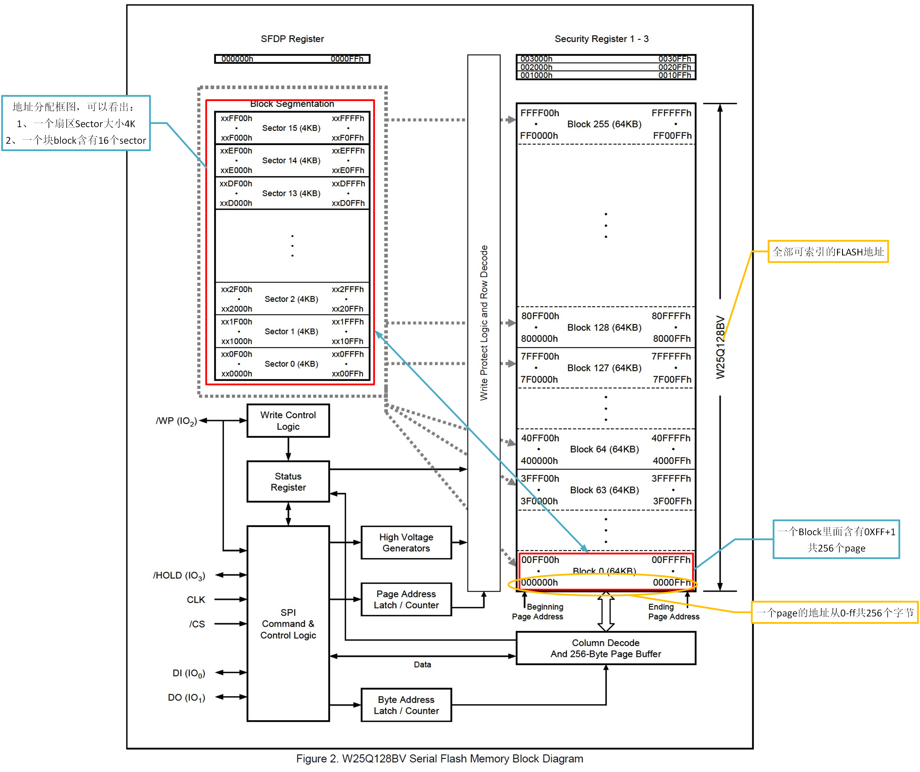
The W25Q128BV array is organized into 65,536 programmable pages of 256-bytes each. Up to 256 bytes can be programmed at a time. Pages can be erased in groups of 16 (4KB sector erase), groups of 128 (32KB block erase), groups of 256 (64KB block erase) or the entire chip (chip erase). The W25Q128BV has 4,096 erasable sectors and 256 erasable blocks respectively. The small 4KB sectors allow for greater flexibility in applications that require data and parameter storage. (See Figure 2.)
The W25Q128BV supports the standard Serial Peripheral Interface (SPI), and a high performance Dual/Quad output as well as Dual/Quad I/O SPI: Serial Clock, Chip Select, Serial Data I/O0 (DI), I/O1 (DO), I/O2 (/WP), and I/O3 (/HOLD). SPI clock frequencies of up to 104MHz are supported allowing equivalent clock rates of 208MHz (104MHz x 2) for Dual Output and 280MHz (70MHz x 4) for Quad SPI when using the Fast Read Quad SPI instructions. These transfer rates can out perform standard Asynchronous 8 and 16-bit Parallel Flash memories. The Continuous Read Mode allows for efficient memory access with as few as 8-clocks of instruction-overhead to read a 24-bit address, allowing true XIP (execute in place) operation.
A Hold pin, Write Protect pin and programmable write protection, with top, bottom or complement array control, provide further control flexibility. Additionally, the device supports JEDEC standard manufacturer and device identification with a 64-bit Unique Serial Number.
W25Q128BV为空间、引脚和电源受限的系统提供存储的解决方案,25Q系列的flash都是NOR Flash,W25Q128BV可编程的页(page)有65536个,每个页256字节(4个页1KB),一次可以访问256字节(一个页)。
页可以一组一组的擦除,每组可以含有16/128/256个页,或者是整片擦除。擦16个页被称作扇区擦除(sector erase),擦128个页被称作块擦除(block erase)。根据定义,可编程的page有65536个,16个page是一个sector,256个page是一个block,因此可被索引到的sector有4096个,block有256个。
通信协议为标准SPI协议,引脚复用可以选择双路或4路SPI通信,同时最大时钟也有不同。另外还包括一个Hold脚,写保护脚,同时有一个64bit,8字节的唯一设备序列号。
关于SPI
常见的SPI通信实现一般包括4根线,CLK,CS,MOSI,MISO,协议的原理比较简单,其实就是在时钟的不同边沿处选择输入还是输出,当选择是输入的时候,数据线要有保持数据的能力;当输出的时候,数据线要能够改变电平来输出数据。
用一张图来说明(随便找的,不一定对)
根据CLK的极性(两个采样沿,空闲时电平是高是低),SPI可以分4种工作模式(CLK的排列组合),这里不介绍工作模式(因为图也不一定对)。主要说一下以下几点
- 无论是哪种模式,当采集的时候,电平要保持住,不采集的时候,电平可以改变
- 由于CLK的存在,采样和变更电平的是要遵守时序的
- 这里注意一下SDI和SDO的流向,当SCLK上升沿时,对主机M是输入,采样阶段,因此SDI数据是保持住的,当SCLK下降沿时,对主机M是输出,SDO是保持状态
从上面的介绍可以看出,实现SPI最少可以只需要2根线,即SCL和SDA,由SCL提供时序,SDA用来传输数据。这时由于一个时钟周期内只能提供两个边沿,因此只能是一个边沿采样,一个边沿输出(改变电平)。
回到W25Q128上:
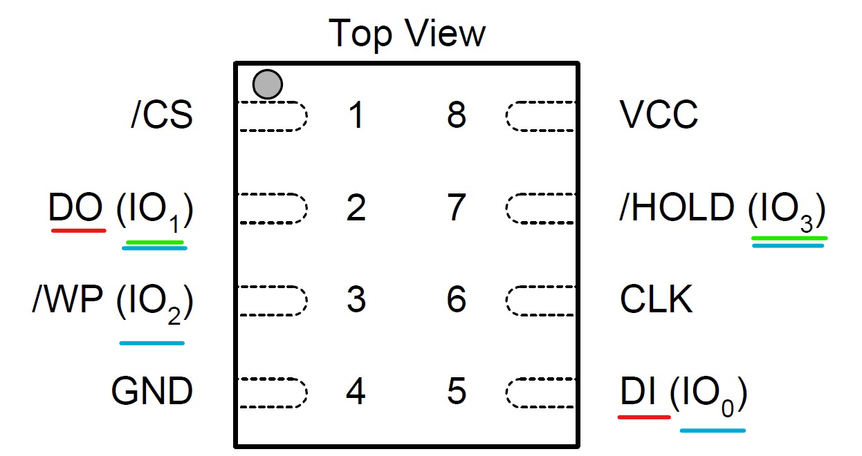
根据手册的引脚定义可以看出有3种使用方式(图片标注有误,以文字为准):
- DI和DO构成SPI的IO线,一收一发,同时写保护和保持脚都能够按原来的功能使用
- DI和DO构成SPI的IO线,但是均作为单路双向IO,实现双路SPI的发送
- HOLD和WP脚被复用至IO脚,这样有4个双向IO脚,实现4路SPI的发送
这里尽管说支持双路和4路SPI,但是由于没有读控和写控,因此其实只能提供被读取的功能,也就是说Flash芯片被设置为S设备而只能被读写而不能发起读写。
我们跳过文档部分关于封装和引脚定义部分的内容,进入引脚描述部分。
引脚描述
这里主要介绍几个引脚,IO,写保护,保持。IO这里由于支持3种多路SPI方式,因此当采用标准SPI时,DI脚输入,在CLK上升沿写入地址或数据,DO在CLK下降沿输出。
写保护和保持均由寄存器2控制,当寄存器2设置为双路或4路时,写保护和保持的原有功能失效。
模块框图
功能描述
SPI标准模式
The W25Q128BV is accessed through an SPI compatible bus consisting of four signals: Serial Clock (CLK), Chip Select (/CS), Serial Data Input (DI) and Serial Data Output (DO). Standard SPI instructions use the DI input pin to serially write instructions, addresses or data to the device on the rising edge of CLK. The DO output pin is used to read data or status from the device on the falling edge of CLK.
SPI bus operation Mode 0 (0, 0) and 3 (1, 1) are supported. The primary difference between Mode 0 and Mode 3 concerns the normal state of the CLK signal when the SPI bus master is in standby and data is not being transferred to the Serial Flash. For Mode 0, the CLK signal is normally low on the falling and rising edges of /CS. For Mode 3, the CLK signal is normally high on the falling and rising edges of /CS.
DI可以写指令,地址或数据,DO可以读数据或状态。工作模式可以是模式0或模式3
SPI双路模式
The W25Q128BV supports Dual SPI operation when using the “Fast Read Dual Output (3Bh)” and “Fast Read Dual I/O (BBh)” instructions. These instructions allow data to be transferred to or from the device at two to three times the rate of ordinary Serial Flash devices. The Dual SPI Read instructions are ideal for quickly downloading code to RAM upon power-up (code-shadowing) or for executing non-speed-critical code directly from the SPI bus (XIP). When using Dual SPI instructions, the DI and DO pins become bidirectional I/O pins: IO0 and IO1.
双路模式在3Bh,BBh指令执行后使用,执行后DI和DO将被设置成双向IO的IO0和IO1。
SPI四路模式
The W25Q128BV supports Quad SPI operation when using the “Fast Read Quad Output (6Bh)”, “Fast Read Quad I/O (EBh)”, “Word Read Quad I/O (E7h)” and “Octal Word Read Quad I/O (E3h)” instructions. These instructions allow data to be transferred to or from the device six to eight times the rate of ordinary Serial Flash. The Quad Read instructions offer a significant improvement in continuous and random access transfer rates allowing fast code-shadowing to RAM or execution directly from the SPI bus (XIP). When using Quad SPI instructions the DI and DO pins become bidirectional IO0 and IO1, and the /WP and /HOLD pins become IO2 and IO3 respectively. Quad SPI instructions require the non-volatile Quad Enable bit (QE) in Status Register-2 to be set.
类似双路,执行6B,EB,E7,E3指令后可以使用4路模式,引脚被复用。四路模式需要状态寄存器2的QE位保持有效不发生改变
其他功能如保持和写保护这里暂时跳过。
状态寄存器和指令
状态寄存器1和状态寄存器2的位定义如图:
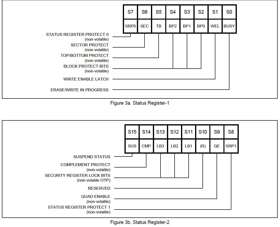
具体的每一位的含义在手册中已经写明,这里说一下这两个寄存器如何访问(用指令来交互的格式):
The instruction set of the W25Q128BV consists of thirty five basic instructions that are fully controlled through the SPI bus (see Instruction Set table1-3). Instructions are initiated with the falling edge of Chip Select (/CS). The first byte of data clocked into the DI input provides the instruction code. Data on the DI input is sampled on the rising edge of clock with most significant bit (MSB) first.
Instructions vary in length from a single byte to several bytes and may be followed by address bytes, data bytes, dummy bytes (don’t care), and in some cases, a combination. Instructions are completed with the rising edge of edge /CS. Clock relative timing diagrams for each instruction are included in Figures 4 through 37. All read instructions can be completed after any clocked bit. However, all instructions that Write, Program or Erase must complete on a byte boundary (/CS driven high after a full 8-bits have been clocked) otherwise the instruction will be ignored. This feature further protects the device from inadvertent writes. Additionally, while the memory is being programmed or erased, or when the Status Register is being written, all instructions except for Read Status Register will be ignored until the program or erase cycle has completed.
从SPI发送的第一个字节就是指令的指令码,根据描述,指令的总长度是变长的,即指令码后面可能跟随着:地址、数据、占位等等。
指令如下表(部分):
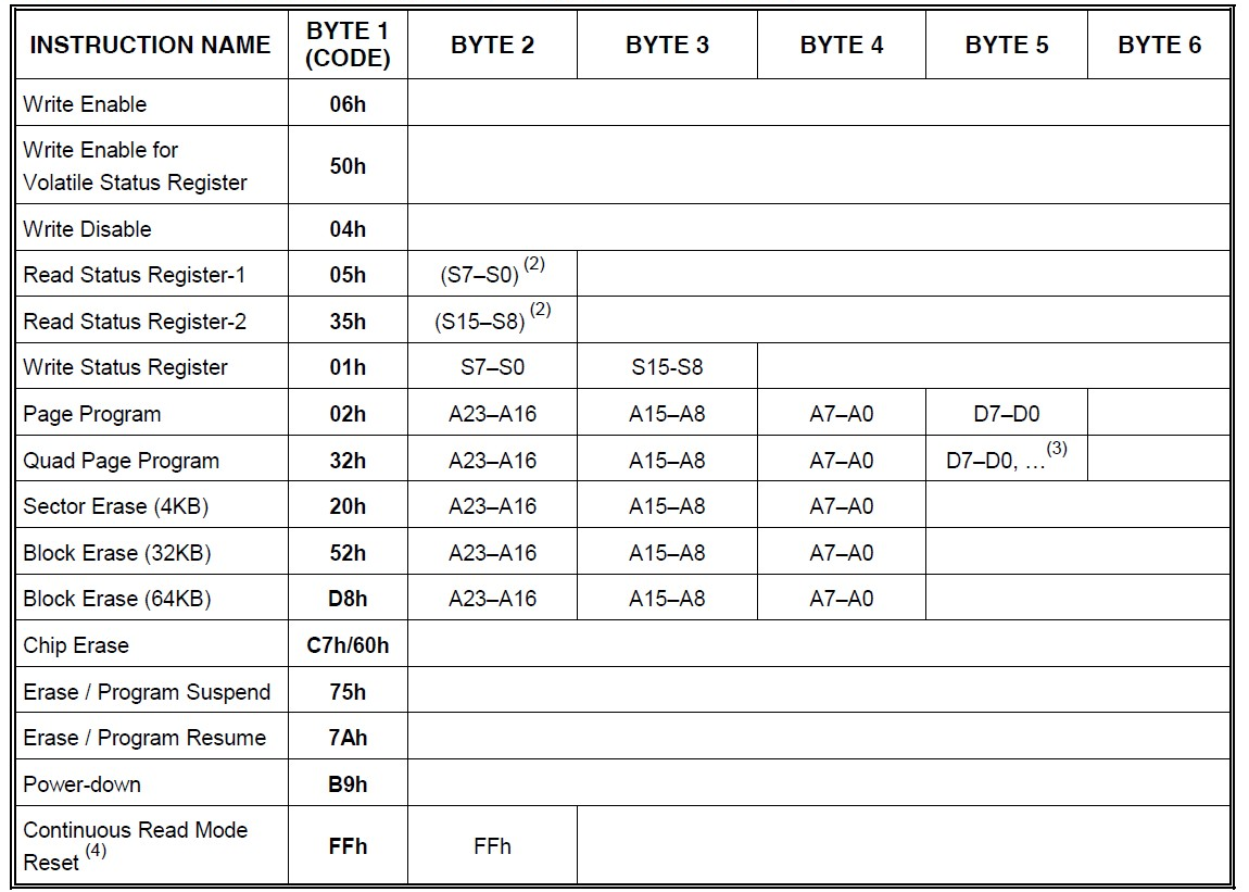
BYTE1的位置表示发送的第一个字节,可以看出大部分都是只发一个字节,05H和35H发送后会收到1个字节的返回值,而01H,02H...D8H发送的数据长度均大于1个字节。注意读写地址线只有24根,即可索引的地址范围为0x00000000-0x00FFFFFF,即16M,刚好索引到全部地址范围。
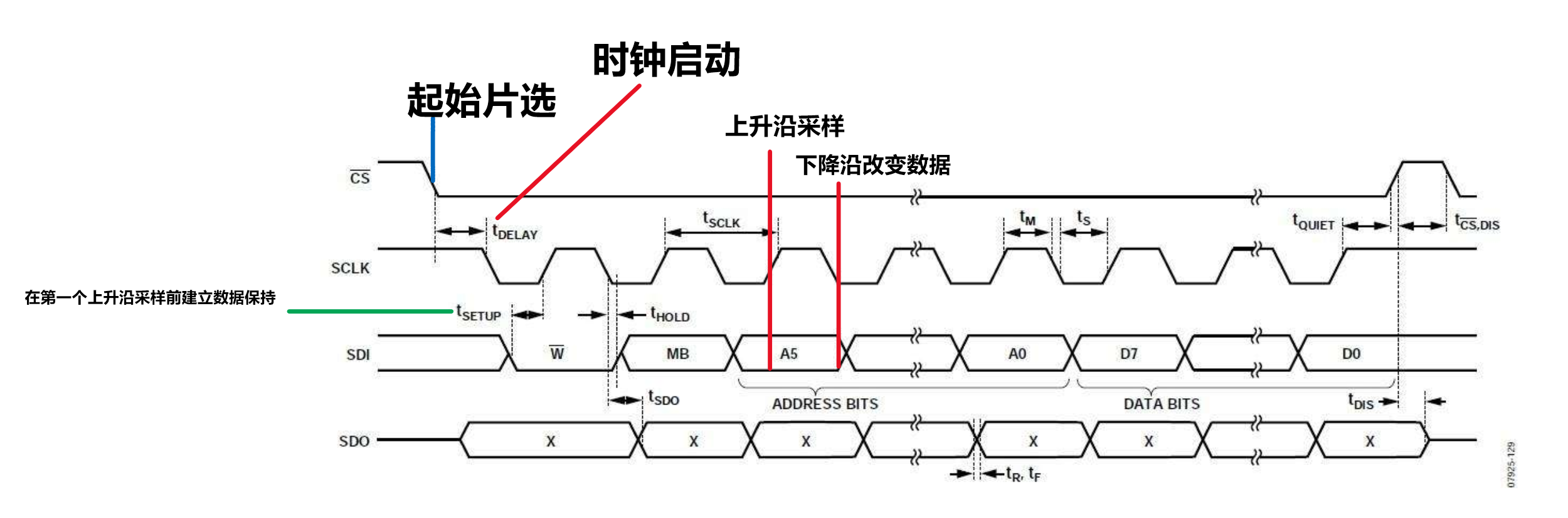
注意02H,之前说到过,手册上写的一次编程大小是一页,即256字节,所以02的指令描述那里其实是BTYE5后面要跟256个字节,这里可能是没有标明。这一点在后面的时序图中也可以得到印证:
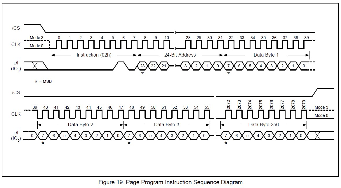
这里吐槽一下,画时序图固然有助于硬件工程师设计,但是应该同时配一组协议格式说明表格一类的文档,便于软件开发,读时序对于简单协议尚能接受,但是对于这种整字节操作应该直接用字节表示更清晰些。后面全部都是指令协议的定义和说明,就不介绍了。