在一个FPGA项目中,全局网络的建立至关重要,其中包括时钟网络和复位网络,通常我们在设计的时候对时钟网络的规划格外小心,却忽视了复位网络,其实复位是需要在设计中考虑和实现的最常见也更重要的控制信号之一,它跟时钟一样也是一个覆盖全局、高扇出的信号,复位会给用户设计的性能、使用面积和功耗产生显著影响,这个复位如果处理不当也会导致意想不到的错误。那么复位信号选择同步还是异步、高电平还是低电平有效?对于这个问题,针对Xilinx 7系列FPGA,就聊一聊这个问题。Xiinx 7系列FPGA推荐使用同步高电平复位,这与我们平时用到的异步低电平复位有很大出入,至于为何如此且听细细道来。
1 什么情况下使用复位信号
很多工程师习惯于对FPGA设计进行上电复位,总担心如果不复位,触发器就处于不定状态,导致系统跑飞。事实上,每个触发器都有明确的初始值,这个初始值与是否复位无关。因此,一旦系统上电,即使没有复位,对于FDSE和FDPE,其初始值为1,对于FDRE和FDCE,其初始值为0。Block RAM和DSP48内部触发器初始值为0。
1.如果只是上电复位,那么这种复位是不需要的
对于控制路径,例如状态机,这种复位通常是必需的。相比之下,数据路径的复位通常是不需要的。因为,老的数据总会被新数据“冲走”
2.通常,控制路径需要复位,数据路径不需要复位
从功能仿真的角度看,如果没有初始值,触发器输出会显示“X”,从而导致仿真无法继续。解决方法是在定义触发器时,给出初始值,如下图所示,而且这种方式是可综合的。
reg a = 1'b0;
3.功能仿真时,为获得触发器初始值,可在定义该触发器时直接声明,无需复位
2 同步复位 vs 异步复位
在官方文档UG949《UltraFast Design Methodology Guide for the Vivado Design Suite》中关于复位有如下一段描述:
Synchronous Reset vs. Asynchronous Reset
If a reset is needed, Xilinx recommends code synchronous resets. Synchronous resets have many advantages over asynchronous resets.
- Synchronous resets can directly map to more resource elements in the FPGA device architecture.
- Asynchronous resets also impact the performance of the general logic structures. As all Xilinx FPGA general-purpose registers can program the set/reset as either asynchronous or synchronous, it can be perceived that there is no penalty in using asynchronous resets. That assumption is often wrong. If a global asynchronous reset is used, it does not increase the control sets. However, the need to route this reset signal to all register elements increases timing complexity.
- If using asynchronous reset, remember to synchronize the deassertion of the asynchronous reset.
- Synchronous resets give more flexibility for control set remapping when higher density or fine tuned placement is needed. A synchronous reset may be remapped to the data path of the register if an incompatible reset is found in the more optimally placed Slice. This can reduce wire length and increase density where needed to allow proper fitting and improved performance.
- Asynchronous resets might require multicycle assertion to ensure a circuit is properly reset and stable. When properly timed, synchronous resets do not have this requirement.
- Use synchronous resets if asynchronous resets have a greater probability of upsetting memory contents to block RAMs, LUTRAMs, and SRLs during reset assertion.
- Some resources such as the DSP48 and block RAM have only synchronous resets for the register elements within the block. When asynchronous resets are used on register elements associated with these elements, those registers may not be inferred directly into those blocks without impacting functionality.
也就是说,在设计中如何开发人员需要使用复位,xilinx建议代码同步复位,并且官方文档中也给出了使用同步复位与异步复位对设计所造成的不同影响。
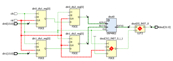
下面的代码使用了异步复位的16X16位的乘法器,综合后的结果如下图,DSP48不支持异步复位,因此,这些触发器均为SLICE中的触发器,这就会额外消耗65个触发器和32个LUT。
module mult (
    input                   clk,
    input                   rst,
    input       [15:0]      din0,
    input       [15:0]      din1,
    output reg  [31:0]      dout
    );

reg [15:0] din0_dly1,din0_dly2;
reg [15:0] din1_dly1,din1_dly2;

always @ (posedge clk or posedge rst) begin
    if  (rst) begin
        din0_dly1 <= 16'h0;
        din0_dly2 <= 16'h0;
        din1_dly1 <= 16'h0;
        din1_dly2 <= 16'h0;
        dout      <= 32'h0;
    end else begin
        din0_dly1 <= din0;
        din0_dly2 <= din0_dly1;
        din1_dly1 <= din1;
        din1_dly2 <= din1_dly1;
        dout      <= din0_dly2 * din1_dly2;
    end
end

endmodule
module mult (
    input                   clk,
    input                   rst,
    input       [15:0]      din0,
    input       [15:0]      din1,
    output reg  [31:0]      dout
    );

reg [15:0] din0_dly1,din0_dly2;
reg [15:0] din1_dly1,din1_dly2;

always @ (posedge clk) begin
    if  (rst) begin
        din0_dly1 <= 16'h0;
        din0_dly2 <= 16'h0;
        din1_dly1 <= 16'h0;
        din1_dly2 <= 16'h0;
        dout      <= 32'h0;
    end else begin
        din0_dly1 <= din0;
        din0_dly2 <= din0_dly1;
        din1_dly1 <= din1;
        din1_dly2 <= din1_dly1;
        dout      <= din0_dly2 * din1_dly2;
    end
end

endmodule

而上图为使用同步复位综合后的结果,上述触发器会完美地映射到DSP48内部,设计对比异步复位的设计具有最佳的资源使用率,更好的性能和更低的功耗,并且逻辑层数也更少。
3 高电平 VS 低电平
在上文描述同步、异步复位的HDL代码中都为高电平有效复位,异步复位只要在判断条件中取个反即可。关于选择高电平有效还是选择低电平有效的复位,不像选择同步还是异步有那么些理论根据,因此有些设计者就根据个人代码编写的喜好来选择是高电平复位还是低电平复位。但是高、低电平复位总是有所区别的。
在手册UG949《UltraFast Design Methodology Guide for the Vivado Design Suite》(v2015.3)中对复位使用高电平还是低电平有如下描述,虽然在后续的版本中删除了这一段描述,但是还是推荐使用高电平复位,这是与7系列器件结构所决定的。
Control Signal Polarity (Active-High vs. Active-Low)
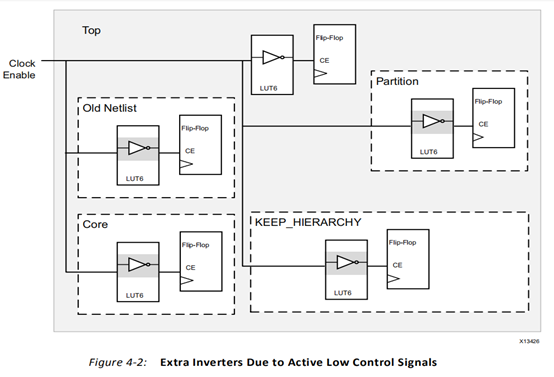
For high-fanout control signals like clock enables or resets, it is best to use active high in the entire design. If a block operates with active low resets or clock enables, inverters get added to the design and there is an associated timing penalty. It can restrict synthesis options to flat or rebuilt to optimize the inverters or require the implementation of a custom solution.
The Slice and internal logic of the Xilinx FPGA clock enables and resets are inherently active-High. Describing active-Low resets or clock enables may result in additional LUTs used as simple inverters for those routes.
For UltraScale devices, a programmable inversion is available on the reset. Therefore, reset polarity is more flexible. However, Xilinx still recommends keeping the reset polarity coding consistent (all active-High or all active-Low) to allow for maximum flexibility for packing logic. The enable does not have an inversion so Xilinx recommends always describing active-High enables.
对于Xilinx 7系列FPGA的结构,其中复位可以通过两种方式实现:全局复位网络(GSR)和普通复位端,如图2所示为7系列FPGA中的Storage Element结构(具体内容参阅“7 Series FPGAs Configurable Logic Block”,ug474),它既可以配置成Flip-Flop也可以配置成Latch,由输入端D、输出端Q,三个控制信号时钟使能CE、时钟CK和置位/复位SR组成;内部还有INIT0、INIT1、SRLO和SRHI 四个选项,其中INIT0和INIT1配对,表示通过GSR全局复位,此复位网络是异步的,并且铺设在整个芯片区域,属于硬核,用户无法自定义修改;而SRLO和SRHI配对,表示高电平有效信号SR驱动的复位,此信号可以配置成异步或者同步,根据此特性,如果使用低电平有效的复位,实现时则需要在SR端额外加入一个非门,因此在7系列FPGA设计时推荐使用高电平有效的复位。
选择高还是低,需要根据具体的电平标准、器件结构来选择,并不是一概而论低电平有效的好或者高电平有效的好。
参考资料
[1]Xilinx,“Get Smart About Reset: Think Local, Not Global ”,wp272(v1.0.1)
[2]Xilinx,“UltraFast Design Methodology Guide for the Vivado Design Suite”,ug949(v2018.1/v2015.3)
[3]Xilinx,“7 Series FPGAs Configurable Logic Block”,ug474(v1.8)
[4]Xilinx,“UltraScale Architecture Libraries Guide”,ug974(v2018.1)
[5]https://www.veryarm.com/173792.html